Comtech EF Data PCB-4000 User Manual
Page 22
PCB-4000 1+1 Phase Combiner
Revision 2
External Connectors
MN/PCB4000.IOM
2–2
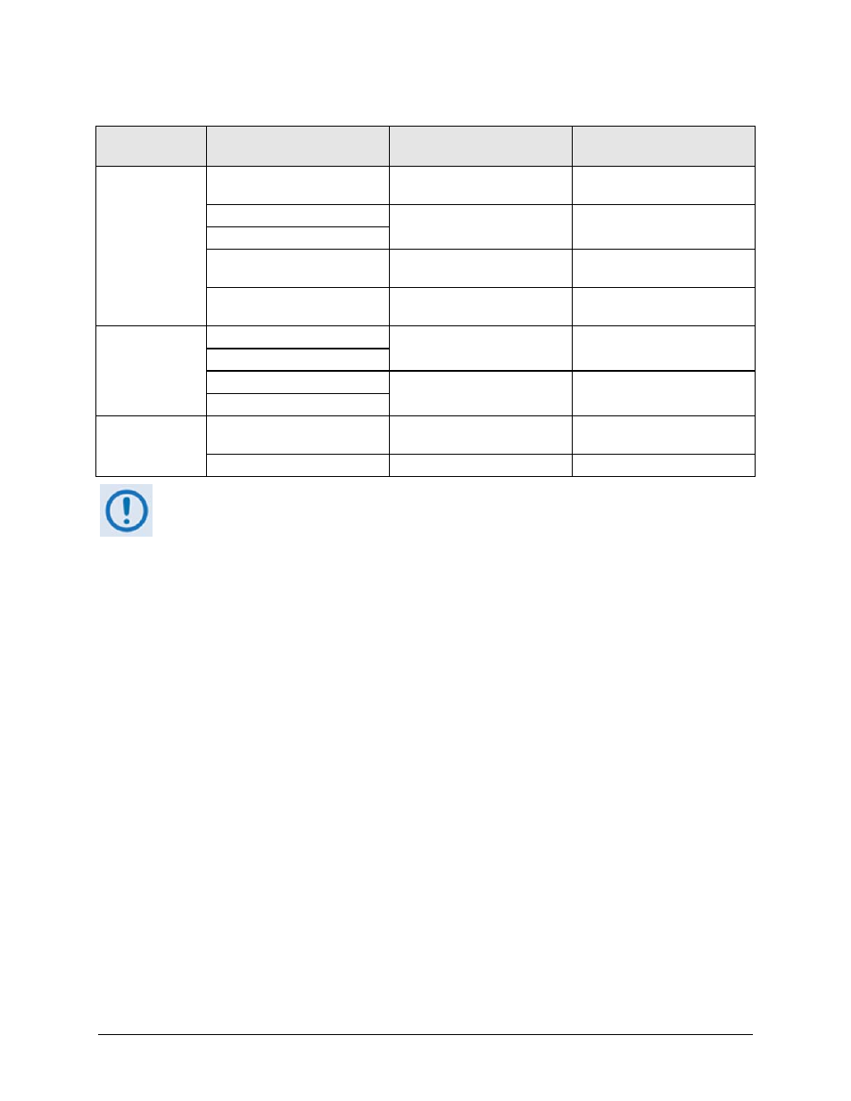
Table 2-1. PCB-4000 External Connectors
Connector Group
(Chapter Sect.)
Name / Ref Des
Connector Type
Function
M&C
(Sect. 2.2)
SYSTEM COM | J1
19-pin Circular Connector
Customer EIA-232/485 and
discrete interface
SSPA COM 1 | J2
19-pin Circular Connector
Connects to SSPAs
SSPA COM 2 | J3
SSPA SW OUT| J5
19-pin Circular Connector
Connects to both waveguide
switches
RF INPUT SWITCH | J6
6-pin Circular Connector
Drive input, selects either RF IN
1 or RF IN 2
RF
(Sect. 2.3)
RF IN 1 | J7
Type ’N’
RF Inputs to PCCB
RF IN 2 | J8
SSPA OUT 1 | J9
Type ’N’
RF Outputs to SSPAs
SSPA OUT 2 | J10
Power/Ground
(Sect 2.4)
AC
Pin ‘R’ on SSPA COM 1 J1,
SSPA COM 2 J3
See Sect. 2.4.1 for AC power
provision note
Ground
#10-32 stud
Common Chassis Ground
To maintain compliance with the European EMC Directive (EN55022, EN50082‐1) properly
shielded cables are required for data I/O.
- CDD-880 (124 pages)
- CDM-800 (130 pages)
- ODMR-840 (184 pages)
- CDM-750 (302 pages)
- CDM-840 (244 pages)
- SLM-5650A (420 pages)
- CTOG-250 (236 pages)
- CDM-700 (256 pages)
- CDM-760 (416 pages)
- CDM-710G (246 pages)
- CDM-600/600L (278 pages)
- CDMR-570L (512 pages)
- CDM-625 (684 pages)
- CDM-625A (756 pages)
- CDD-564A (240 pages)
- CDD-564L (254 pages)
- CLO-10 (134 pages)
- MCED-100 (96 pages)
- CDMR-570AL (618 pages)
- CDM-600 LDPC (2 pages)
- BUC Power Supply Ground Cable (2 pages)
- MPP70 Hardware Kit for CDM-570L (4 pages)
- MPP50 Hardware Kit for CDM-570L (4 pages)
- CDM-625 DC-AC Conversion (4 pages)
- CDM-625 DC-AC Conversion with IP Packet Processor (4 pages)
- DMDVR20 LBST Rev 1.1 (117 pages)
- DMD2050E (212 pages)
- DMD-2050 (342 pages)
- DMD1050 (188 pages)
- OM20 (220 pages)
- QAM256 (87 pages)
- DD240XR Rev Е (121 pages)
- MM200 ASI Field (5 pages)
- DM240-DVB (196 pages)
- MM200 (192 pages)
- CRS-150 (78 pages)
- CRS-280L (64 pages)
- CRS-170A (172 pages)
- CRS-180 (136 pages)
- SMS-301 (124 pages)
- CiM-25/8000 (186 pages)
- CiM-25 (26 pages)
- CRS-500 (218 pages)
- CRS-311 (196 pages)
- CIC-20 LVDS to HSSI (26 pages)