Introduction sorensen sld-series dc load, Figure 1-12 sld-series block diagram, Ia ib com com chan.a chan.b – AMETEK SLD Series User Manual
Page 20

Introduction
Sorensen SLD-Series DC Load
1-8
M540075-01 Rev C
IA
IB
COM
COM
CHAN.A
CHAN.B
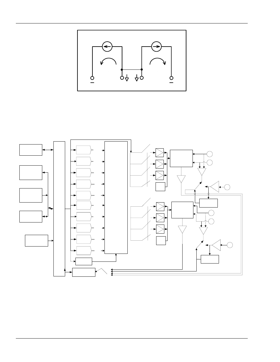
Figure 1-11 SLD-62-xxx-xxx: Dual Negative Load Channel
The system functional block diagram of SLD-series Electronic Load module is illustrated in
Figure 1-12. The functional block diagram of the mainframe is described in the SLM
mainframe operation manuals.
Memory
Front Panel
Display and
Keyboard
OTP Protection
Circuitry
Serial Port
Osciallator Circuit
CPU
16-bit A/D
DVM/DAM
12-bit
D/A
12-bit
D/A
8-bit
D/A
16-bit
D/A
Timer
Dynamic Function
Control
LOW
LEVEL
HIGH
LEVEL
SLEW
RATE
T
HIGH
Load ON
Control
Power MOSFET
Stage
Current
Sense
CC
CR
CV
LOAD
INPUT
Vsense
Control Circuit
Vsense
Input
DVM/DAM
Select
MODE Select
Range
I/II
Power MOSFET
Stage
Current
Sense
CC
CR
CV
LOAD
INPUT
Vsense
Input
MODE Select
Range
I/II
CHANNEL A
CHANNEL B
16-bit
D/A
Timer
T
LOW
12-bit
D/A
12-bit
D/A
8-bit
D/A
16-bit
D/A
Timer
LOW
LEVEL
HIGH
LEVEL
SLEW
RATE
T
HIGH
16-bit
D/A
Timer
T
LOW
Vsense
Control Circuit
Figure 1-12 SLD-series Block Diagram
Each load channel receives the load levels and load status from the chassis via either serial
optical isolated bus or keyboard.
• two 12-bit D/A converters receive digital data of the high and low load levels and
transfer them as an analog signal to the Dynamic Function Generator (DFG)
• two 8-bit D/A converters control the load current slew rate and feed into the DFG
