2085-ow8 and 2085-ow16 i/o data mapping, Analog i/o data mapping, 2085-if4 i/o data mapping – Rockwell Automation 2085 Micro800 Discrete and Analog Expansion I/O Modules User Manual
Page 66: 2085-if8 i/o data mapping
58
Rockwell Automation Publication 2080-UM003A-EN-E - March 2013
Appendix B Expansion I/O Data Mapping
2085-OW8 and 2085-OW16 I/O Data Mapping
Discrete output states can be read from Global Variables _IO_Xx_ST_yy, where
“x” represents the expansion slot number 1…4 and yy represents the point number
00…07 for 2085-OW8 and 00…15 for 2085-OW16.
Discrete output states can be written to Global Variables _IO_Xx_DO_yy, where
“x” represents the expansion slot number 1…4 and yy represents the point number
00…07 for 2085-OW8 and 00…15 for 2085-OW16.
Analog I/O Data Mapping
The following sections provide I/O and status mapping for the following analog
expansion I/O modules:
2085-IF4 I/O Data Mapping
Analog input values are read from Global Variables _IO_Xx_AI_yy, where “x”
represents the expansion slot number 1…4 and yy represents the channel number
00…03.
Analog input status values can be read from Global Variables IO_Xx_ST_yy,
where “x” represents the expansion slot number 1…4 and yy represents the status
word number 00…02.
2085-IF8 I/O Data Mapping
Analog input values are read from Global Variables _IO_Xx_AI_yy, where “x”
represents the expansion slot number 1…4 and yy represents the channel number
00…07.
Catalog Number
Description
2085-IF4
4-channel, 14-bit analog voltage/current input module
2085-IF8
8-channel, 14-bit analog voltage/current input module
2085-OF4
4-channel, 12-bit analog voltage/current output module
2085-IRT4
4-channel, 16-bit RTD and Thermocouple input module
TIP
Use the Connected Components Workbench software to see
Global Variables.
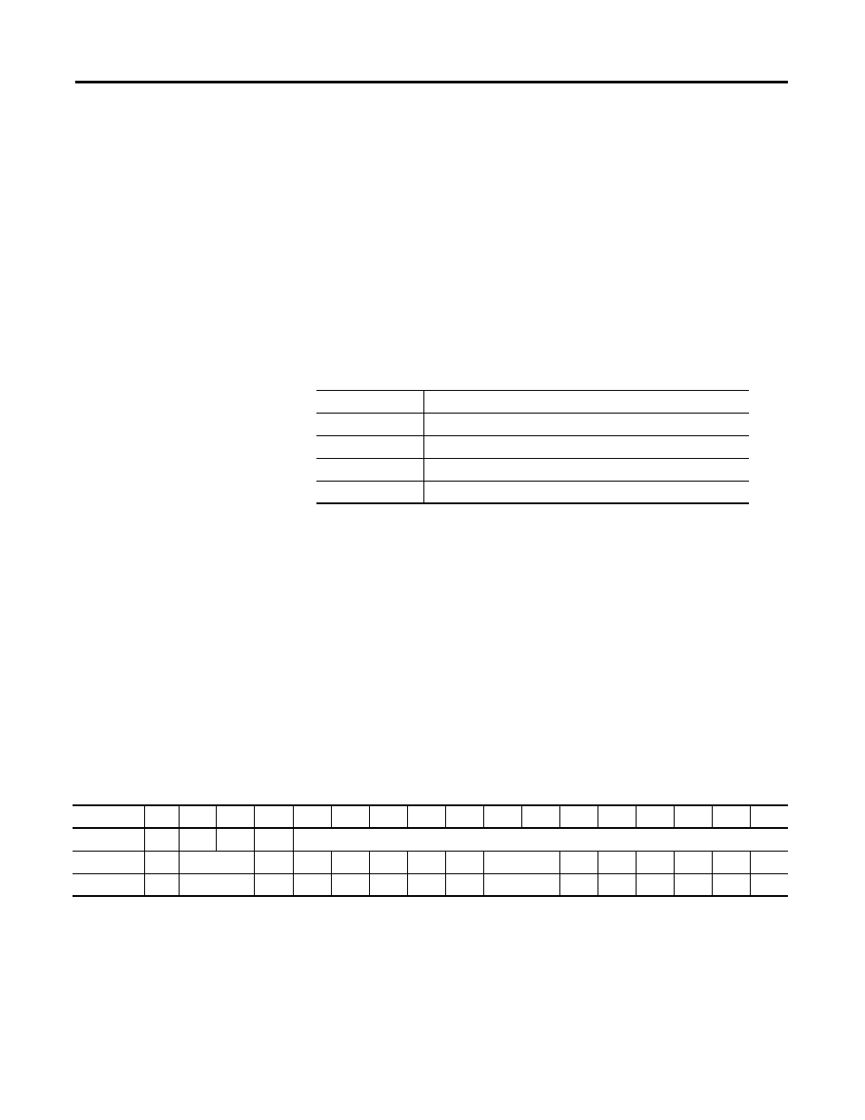
2085-IF4
(1)
Status Data Mapping
Word
R/W
15
14
13
12
11
10
9
8
7
6
5
4
3
2
1
0
Status 0
R
PU
GF
CRC
Reserved
Status 1
R
Reserved
HHA1 LLA1
HA1
LA1
DE1
S1
Reserved
HHA0 LLA0
HA0
LA0
DE0
S0
Status 2
R
Reserved
HHA3 LLA3
HA3
LA3
DE3
S3
Reserved
HHA2 LLA2
HA2
LA2
DE2
S2
(1) See Field Descriptions table for definition of each bit.