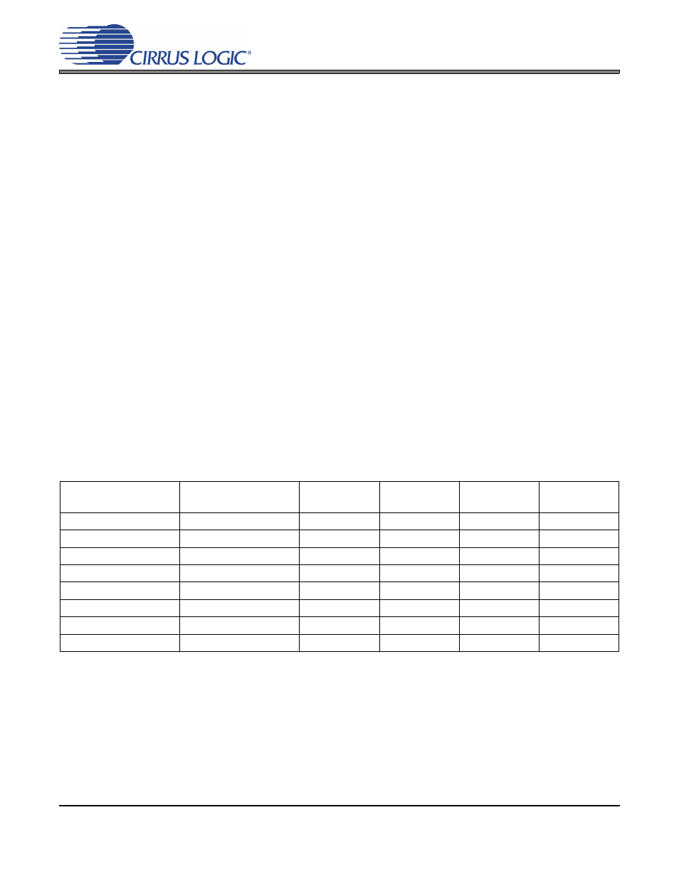
3 hardware mode, 2 omck system clock mode, Table 2. clock switching output clock rates – Cirrus Logic CS8416 User Manual
Page 28: 3 clock recovery and pll filter, Omck system, Cs8416
28
DS578F3
CS8416
The second output of the input multiplexer is used to provide the selected input as a source to be output
on a GPO pin. This pass through signal is selected by TXSEL[2:0] in control port register 04h. This single-
ended signal is resolved to full-rail, but is not de-jittered before it is output.
8.1.3
Hardware Mode
In Hardware Mode the input to the decoder is selected by dedicated pins, RXSEL[1:0].
The pass through signal is selected by dedicated pins, TXSEL[1:0] for output on the dedicated TX pin.
This single-ended signal is resolved to full-rail, but is not de-jittered before it is output.
Selectable inputs are restricted to RXP0 to RXP3 for both the receiver and the TX output pin. These inputs
are selected by RXSEL[1:0] and TXSEL[1:0] respectively.
8.2
OMCK System Clock Mode
A special clock switching mode is available that allows the OMCK clock input to automatically replace
RMCK when the PLL becomes unlocked. This is accomplished without spurious transitions or glitches on
RMCK. In Hardware Mode this feature is enabled by a transition (rising edge active) on the OMCK pin after
reset. Therefore to not enable the clock switching feature in Hardware Mode, OMCK should be tied to DGND
or VL. However, in Hardware Mode, once the clock switching feature has been enabled, it can only be dis-
abled by resetting the part. In Software Mode the automatic clock switching feature is enabled by setting
SWCLK bit in Control1 register to a “1”. Additionally in Software Mode, OMCK can be manually forced to
output on RMCK by using the FSWCLK bit in the Control0 register.
When the clock switching feature is enabled, OSCLK and OLRCK are derived from the OMCK input when
the clock has been switched and the serial port is in master mode. When clock switching is enabled and the
PLL is not locked, OLRCK will be OMCK/256 and OSCLK will be OMCK/4. When the PLL loses lock, the
frequency of the VCO drops to ~750 kHz. When this system clock mode is not enabled, the OSCLK and
OLRCK will be based on the VCO when the PLL is not locked and has reached its steady-state idle frequen-
cy.
shows an example of output clocks based on clock switching being enabled or disabled.
8.3
Clock Recovery and PLL Filter
Please see
for a general description of the PLL, selection of recommended PLL filter
components, and layout considerations.
show the recommended configuration of the two
capacitors and one resistor that comprise the PLL filter.
Clock Switching
Enabled/Disabled
PLL
Locked/Unlocked
RMCK Clock
Ratio
RMCK
OSCLK
OLRCK
Disabled
Locked
128*F
s
6.144 MHz
3.072 MHz
48 kHz
Enabled
Locked
128*F
s
6.144 MHz
3.072 MHz
48 kHz
Disabled
Unlocked
128*F
s
~375 kHz
~187.5 kHz
~2.925 kHz
Enabled
Unlocked
128*F
s
11.2896 MHz
2.8224 MHz
44.1 kHz
Disabled
Locked
256*F
s
12.288 MHz
3.072 MHz
48 kHz
Enabled
Locked
256*F
s
12.288 MHz
3.072 MHz
48 kHz
Disabled
Unlocked
256*F
s
~750 kHz
~187.5 kHz
~2.925 kHz
Enabled
Unlocked
256*F
s
11.2896 MHz
2.8224 MHz
44.1 kHz
Example with OMCK = 11.2896 MHz, the receiver input sample rate = 48 kHz,
OSLCK = 64*Fs, and FSWCLK (Software Mode only) = ‘0’.
Table 2. Clock Switching Output Clock Rates