Cs8416 – Cirrus Logic CS8416 User Manual
Page 13
DS578F3
13
CS8416
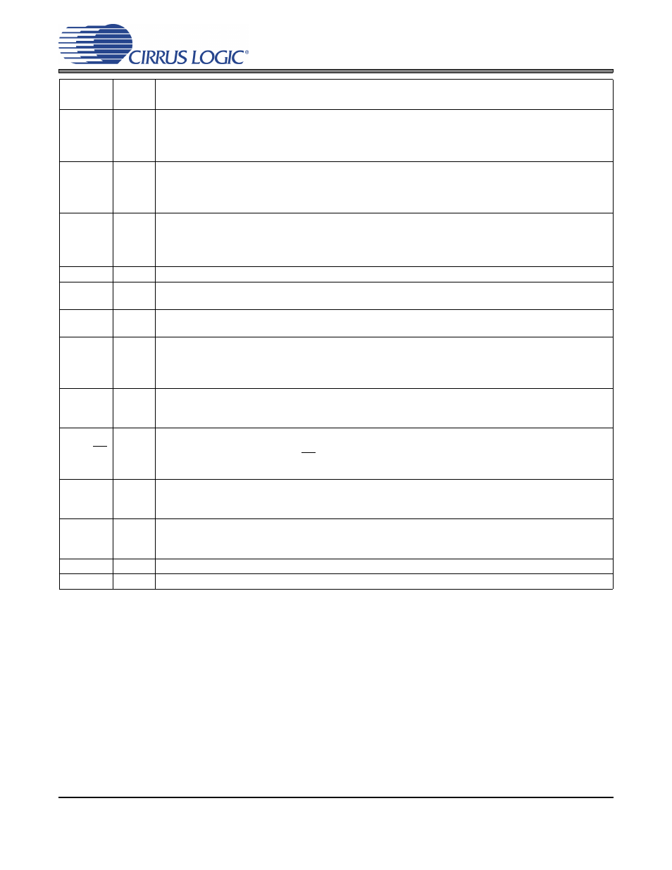
RXN
5
Negative AES3/SPDIF Input (Input) - Single-ended or differential receiver input carrying AES3 or
S/PDIF encoded digital data. Used along with RXP[7:0] to form an AES3 differential input. In single-
ended operation this should be AC coupled to ground through a capacitor. See
AES3/SPDIF/IEC60958 Receiver Components” on page 49
for recommended input circuits.
OMCK
25
System Clock (Input) - When the OMCK System Clock Mode is enabled using the SWCLK bit in the
Control 1 register, the clock signal input on this pin is automatically output through RMCK on PLL unlock.
OMCK serves as the reference signal for OMCK/RMCK ratio expressed in register 18h.
Clock Mode” section on page 28
RMCK
24
Input Section Recovered Master Clock (Output) - Input section recovered master clock output from
the PLL. Frequency defaults to 256x the sample rate (F
s
) and may be set to 128x through the RMCKF bit
in the Control 1 register (01h). RMCK may also be set to high impedance by the RXD bit in the Control 4
register (04h).
OSCLK
27
Serial Audio Output Bit Clock (Input/Output) - Serial bit clock for audio data on the SDOUT pin
OLRCK
28
Serial Audio Output Left/Right Clock (Input/Output) - Word rate clock for the audio data on the
SDOUT pin. Frequency will be the output sample rate (Fs)
SDOUT
26
Serial Audio Output Data (Output) - Audio data serial output pin. This pin must be pulled high to VL
through a 47 k
Ω resistor to place the part in Software Mode.
SDA /
CDOUT
17
Serial Control Data I/O (I²C) / Data Out (SPI) (Input/Output) - In I²C Mode, SDA is the control I/O data
line. SDA is open drain and requires an external pull-up resistor to VL. In SPI Mode, CDOUT is the out-
put data from the control port interface on the CS8416. See the
“Control Port Description” section on
.
SCL /
CCLK
16
Control Port Clock (Input) - Serial control interface clock and is used to clock control data bits into and
out of the CS8416. CCLK is an open drain output and requires an external pull-up resistor to VL. See the
“Control Port Description” section on page 33
AD0 / CS
14
Address Bit 0 (I²C) / Control Port Chip Select (SPI) (Input) - A falling edge on this pin puts the CS8416
into SPI Control Port Mode. With no falling edge, the CS8416 defaults to I²C Mode. In I²C Mode, AD0 is
a chip address pin. In SPI Mode, CS is used to enable the control port interface on the CS8416. See the
“Control Port Description” section on page 33
AD1 /
CDIN
15
Address Bit 1 (I²C) / Serial Control Data in (SPI) (Input) - In I²C Mode, AD1 is a chip address pin. In
SPI Mode, CDIN is the input data line for the control port interface. See the
AD2 /
GPO2
18
General Purpose Output 2 (Output) - If using the I²C control port, this pin must be pulled high or low
through a 47 k
Ω resistor. See the
“Control Port Description” section on page 33
for GPO functions.
GPO1
19
General Purpose Output 1 (Output) - See
“General Purpose Outputs” on page 29
for GPO functions.
GPO0
20
General Purpose Output 0 (Output) - See
“General Purpose Outputs” on page 29
for GPO functions.
Pin
Name
Pin #
Pin Description