3 voltage reference, 4 crystal oscillator, Figure 1. oscillator connections – Cirrus Logic CS5490 User Manual
Page 7: 2 digital pins, 1 reset input, 2 digital output, 3 uart serial interface, 1 uart, Figure 2. uart serial frame format, 4 mode pin
CS5490
DS982F3
7
2.1.3 Voltage Reference
The CS5490 generates a stable voltage reference of
2.4V between the VREF
pins. The reference system
also requires a filter capacitor of at least 0.1µF between
the VREF
pins.
The reference system is capable of providing a
reference for the CS5490 but has limited ability to drive
external circuitry. It is strongly recommended that
nothing other than the required filter capacitor is
connected to the VREF
pins.
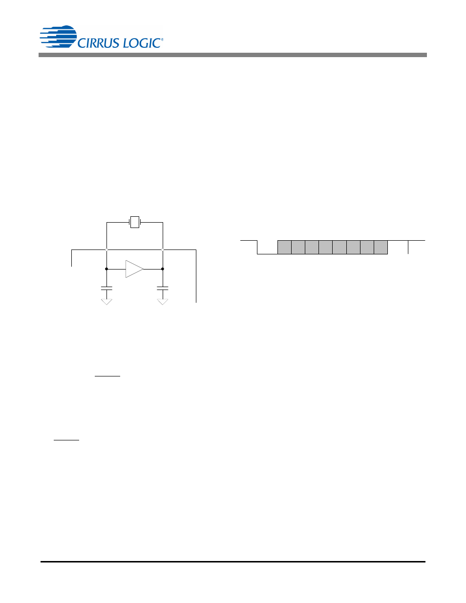
2.1.4 Crystal Oscillator
An external, 4.096MHz quartz crystal can be connected
to the XIN and XOUT pins as shown in
. To re-
duce system cost, each pin is supplied with an on-chip
load capacitor.
Alternatively, an external clock source can be
connected to the XIN pin.
2.2 Digital Pins
2.2.1 Reset Input
The active-low RESET pin, when asserted for longer
than 120µs, will halt all CS5490 operations and reset
internal hardware registers and states. When
de-asserted, an initialization sequence begins, setting
the default register values. To prevent erroneous,
noise-induced resets to the part, an external pull-up
resistor and a decoupling capacitor are necessary on
the RESET pin.
2.2.2 Digital Output
The CS5490 provides a configurable digital output
(DO). It can be configured to output energy pulses,
interrupt, zero-crossings, or energy directions. Refer to
the description of the Config1 register in section
on page 32 for more details.
2.2.3 UART Serial Interface
The CS5490 provides two pins, RX and TX, for
communication between a host microcontroller and the
CS5490.
2.2.3.1 UART
The CS5490 provides a two-wire, asynchronous,
full-duplex UART port. The CS5490 UART operates in
8-bit mode, which transmits a total of 10 bits per byte.
Data is transmitted and received LSB first, with one start
bit, eight data bits, and one stop bit.
Figure 2. UART Serial Frame Format
The baud rate is defined in the SerialCtrl register. After
chip reset, the default baud rate is 600, if MCLK is
4.096MHz. The baud rate is based on the contents of
bits BR[15:0] in the SerialCtrl register and is calculated
as follows:
BR[15:0] = Baud Rate x (524288/MCLK)
or
Baud Rate = BR[15:0] / (524288/MCLK)
The maximum baud rate is 512K if MCLK is 4.096MHz.
The UART has two signals: TX and RX. TX is the serial
data output from the CS5490; RX is the serial data input
to the CS5490.
2.2.4 MODE Pin
The MODE pin must be tied to VDDA for normal
operation. The MODE pin is used primarily for factory
test procedures.
XIN
XOUT
C1 = 22pF
C2 = 22pF
Figure 1. Oscillator Connections
0
1
2
7
IDLE
STOP
3
4
5
6
START
DATA
IDLE