Pin description, Clock generator, Control pins and serial data i/o – Cirrus Logic CS5490 User Manual
Page 6: Analog inputs/outputs, Power supply connections, 1 analog pins, 1 voltage input, 2 current input, 1 voltage input 2.1.2 current input, Cs5490

CS5490
6
DS982F3
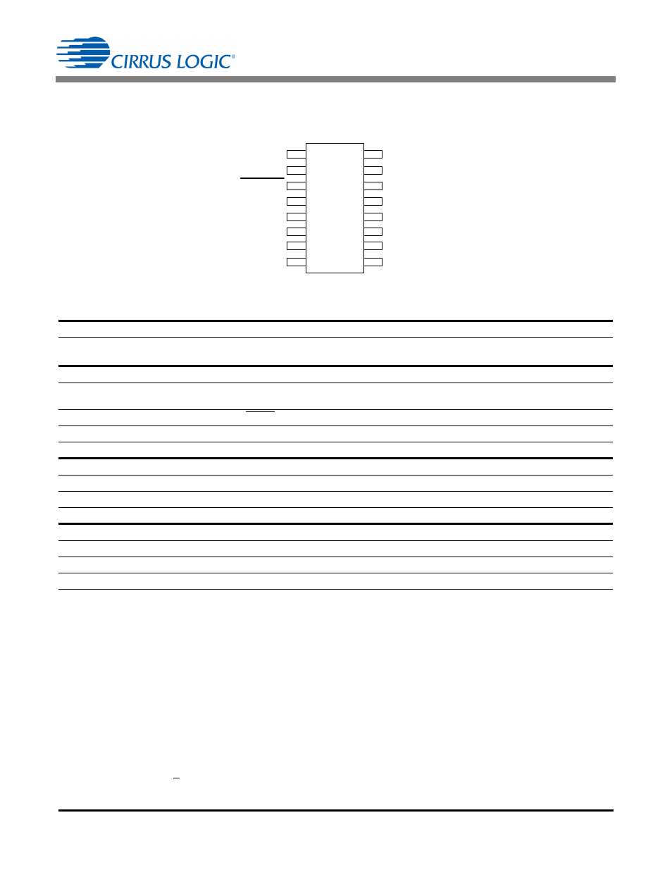
2. PIN DESCRIPTION
2.1 Analog Pins
The CS5490 has two differential inputs, one for voltage
(VIN
) and one for currentIIN). The CS5490 also has
two voltage reference pins (VREF
) between which a
0.1µ bypass capacitor must be placed.
2.1.1 Voltage Input
The output of the line voltage resistive divider or
transformer is connected to the VIN
input of the
CS5490. The voltage channel is equipped with a 10x,
fixed-gain amplifier. The full-scale signal level that can
be applied to the voltage channel is ±250 mV. If the
input signal is a sine wave, the maximum RMS
voltage is 250mVp /
2
176.78mV
RMS
, which is
approximately 70.7% of maximum peak voltage.
2.1.2 Current Input
The output of the current-sensing shunt resistor or
transformer is connected to the IIN
input pins of the
CS5490. To accommodate different current-sensing
elements, the current channel incorporates a
programmable gain amplifier (PGA) with two selectable
input gains, as described in the Config0 register
description
6.6.1 Configuration 0 (Config0) – Page 0,
on page 32. There is a 10x gain setting and
a 50x gain setting. The full-scale signal level for the
current channel is ±50mV and ±250mV for 50x and 10x
gain settings, respectively. If the input signal is a sine
wave, the maximum RMS voltage is 35.35 mV
RMS
or
176.78mV
RMS
, which is approximately 70.7% of
maximum peak voltage.
Clock Generator
Crystal In
Crystal Out
2,1
XIN, XOUT — Connect to an external quartz crystal. Alternatively, an external clock can be
supplied to the XIN pin to provide the system clock for the device.
Control Pins and Serial Data I/O
Digital Output
12
DO — Configurable digital output for energy pulses, interrupt, energy direction, and
zero-crossings.
Reset
3
RESET — An active-low Schmitt-trigger input used to reset the chip.
Serial Interface
13,14
TX, RX — UART serial data output/input.
Operating Mode Select
15
MODE — Connect to VDDA for proper operation.
Analog Inputs/Outputs
Voltage Input
6,7
VIN+, VIN- — Differential analog input for the voltage channel.
Current Input
5,4
IIN+, IIN- — Differential analog input for the current channel.
Voltage Reference Input
9,8
VREF+, VREF- — The voltage reference output and return.
Power Supply Connections
Internal Digital Supply
16
VDDD — Decoupling pin for the internal digital supply.
Positive Analog Supply
11
VDDA — The positive analog supply.
Analog Ground
10
GNDA — Analog ground.
1
7
6
5
4
3
2
8
16
10
11
12
13
14
15
9
XOUT
VREF-
VIN-
VIN+
IIN+
IIN-
RESET
XIN
VDDD
VREF+
GNDA
VDDA
DO
TX
RX
MODE
