Functional description, 1 power-on reset (por), Figure 8. power-on reset timing – Cirrus Logic CS5490 User Manual
Page 18: Table 1. por thresholds, 2 power saving modes, 3 zero-crossing detection, Cs5490
CS5490
18
DS982F3
5. FUNCTIONAL DESCRIPTION
5.1 Power-on Reset (POR)
The CS5490 has an internal power supply supervisor
circuit that monitors the VDDA and VDDD power
supplies and provides the master reset to the chip. If
any of these voltages are in the reset range, the master
reset is triggered.
Both the analog and the digital supply have their own
POR circuit. During power-up, both supplies have to be
above the rising threshold for the master reset to be
de-asserted.
Each POR is divided into 2 blocks: rough and fine.
Rough POR triggers the fine POR. Rough POR
depends only on the supply voltage. The trip point for
the fine POR is dependent on bandgap voltage for
precise control.
The POR circuit also acts as a brownout detect. The fine
POR detects supply drops and asserts the master reset.
The rough and fine PORs have hysteresis in their rise
and fall thresholds which prevents the reset signal from
chattering.
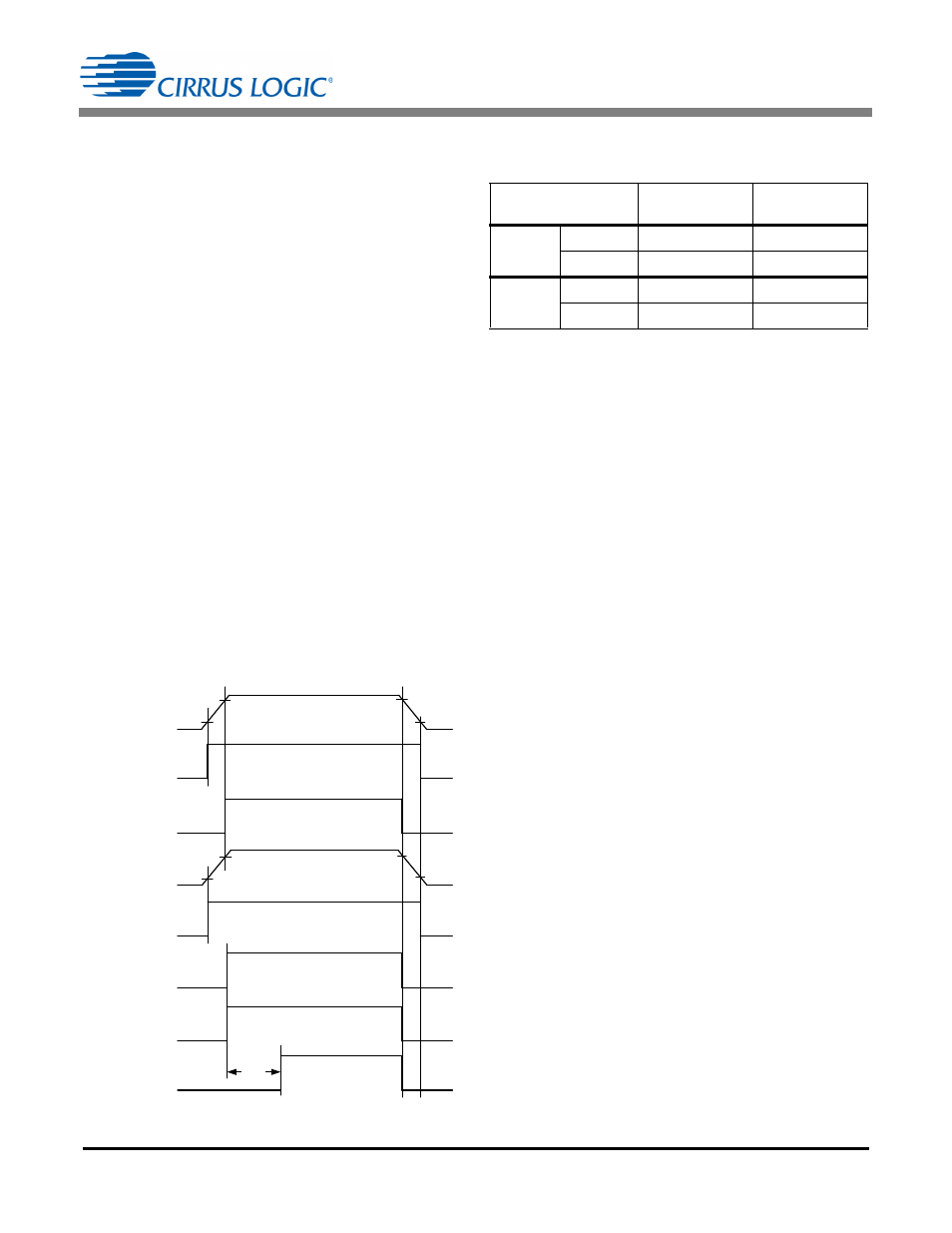
The following plot shows the POR outputs for each of
the power supplies. The POR_Fine_VDDA and
POR_Fine_VDDD signals are AND-ed to form the
actual power-on reset signal to the digital circuity. The
digital circuitry, in turn, holds the master reset signal for
130ms and then de-asserts the master reset.
Figure 8. Power-on Reset Timing
Table 1. POR Thresholds
5.2 Power Saving Modes
Power Saving modes for CS5490 are accessed through
the Host Instruction Commands (see
• Standby: Powers down all the ADCs, rough buffer,
and the temperature sensor. Standby mode disables
the system time calculations. Use the wake-up
command to come out of standby mode.
• Wake-up: Clears the ADC power-down bits and
starts the system time calculations.
After any of these commands are completed, the DRDY
bit is set in the Status0 register.
5.3 Zero-crossing Detection
Zero-crossing detection logic is implemented in
CS5490. A low-pass filter can be enabled by setting
ZX_LPF bit in register Config2. The low-pass filter has
a cut-off frequency of 80Hz. It is used to eliminate any
harmonics and to help the zero-crossing detection on
the 50Hz or 60Hz fundamental component. The
zero-crossing level registers are used to set the
minimum threshold over which the channel peak has to
exceed in order for the zero-crossing detection logic to
function. There are two separate zero-crossing level
registers: VZX
LEVEL
is the threshold for the voltage
channels, and IZX
LEVEL
is the threshold for the current
channels.
VDDA
POR_Rough_VDDA
POR_Fine_VDDA
VDDD
POR_Rough_VDDD
POR_Fine_VDDD
POR_Fine_VDDA
POR_Fine_VDDD
Master Reset
130ms
V
th1
V
th2
V
th5
V
th6
V
th3
V
th4
V
th7
V
th8
Typical POR
Threshold
Rising
Falling
VDDA
Rough
V
th1
= 2.34V
V
th6
= 2.06V
Fine
V
th2
= 2.77V
V
th5
= 2.59V
VDDD
Rough
V
th3
= 1.20V
V
th8
= 1.06V
Fine
V
th4
= 1.51V
V
th7
= 1.42V