8 temperature measurement, 9 anti-creep, 10 register protection – Cirrus Logic CS5490 User Manual
Page 23: 1 write protection, 2 register checksum, 9 anti-creep 5.10 register protection, 1 write protection 5.10.2 register checksum, Figure 13, Illustrate, Are illustrated in
CS5490
DS982F3
23
5.8 Temperature Measurement
The CS5490 has an internal temperature sensor, which
is designed to measure temperature and optionally
compensate for temperature drift of the voltage
reference. Temperature measurements are stored in
the temperature register (T), which, by default, is
configured to a range of ±128°C.
The application program can change the scale and
range of the temperature (T) register by changing the
temperature gain (T
GAIN
) register and temperature
offset (T
OFF
) register.
The temperature (T) register updates every 2240 output
word rate (OWR) samples. The Status0 register bit TUP
indicates when T is updated.
5.9 Anti-creep
The anti-creep (no-load threshold) is used to determine
if a no-load condition is detected. The |P
Sum
| and |Q
Sum
|
are compared to the value in the no-load threshold
(Load
Min
) register. If both |P
Sum
| and |Q
Sum
| are less
than this threshold, then P
Sum
and Q
Sum
are forced to
zero. If S
Sum
is less than the value in Load
Min
register,
then S
Sum
is forced to zero.
5.10 Register Protection
To prevent the critical configuration and calibration
registers from unintended changes, the CS5490 provides
two enhanced register protection mechanisms: write
protection and automatic checksum calculation.
5.10.1 Write Protection
Setting the DSP_LCK[4:0] bits in the RegLock register
to 0x16 enables the CS5490 DSP lockable registers to
be write-protected from the calculation engine. Setting
the DSP_LCK[4:0] bits to 0x09 disables the
write-protection mode.
Setting the HOST_LCK[4:0] bits in the RegLock register
to 0x16 enables the CS5490 HOST lockable registers to
be write-protected from the serial interface. Setting the
HOST_LCK[4:0] bits to 0x09 disables the
write-protection mode.
For registers that are DSP lockable, HOST lockable, or
both, refer to sections
on page 28, and
5.10.2 Register Checksum
All the configuration and calibration registers are
protected by checksum, if enabled. Refer to sections
Hardware Registers Summary (Page 0)
Software Registers Summary (Page 16)
and
6.4 Software Registers Summary (Page 17)
page 30. The checksum for all registers marked with an
asterisk symbol (*) is computed at the rate of OWR. The
checksum result is stored in the RegChk register. After
the CS5490 has been fully configured and loaded with
the calibrations, the host microcontroller should keep a
copy of the checksum (RegChk_Copy) in its memory. In
normal operation, the host microcontroller can read the
RegChk register and compare it with the saved copy of
the RegChk register. If the two values mismatch, a reload
of configurations and calibrations into the CS5490 is
necessary.
The automatic checksum computation can be disabled by
setting the REG_CSUM_OFF bit in the Config2 register.
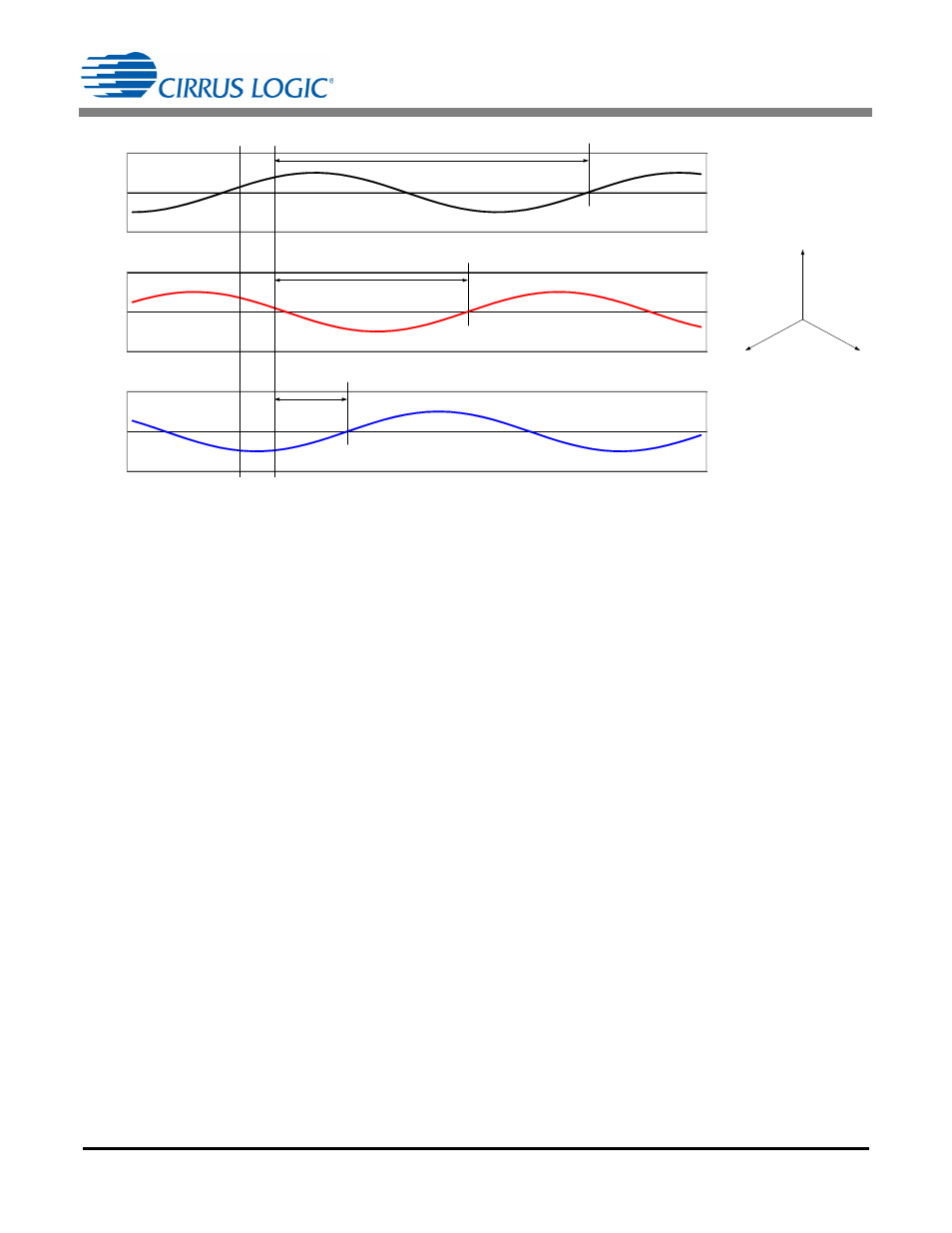
-2
0
2
Phase A Channel
-2
0
2
Phase B Channel
-2
0
2
Phase C Channel
Stop
Stop
Stop
Phase C Count
Phase B Count
Phase A Count
A
B
C
Write 0x16 to
PSDC Register
Start on the Falling
Edge on the RX Pin
Figure 13. Phase Sequence C, B, A for Rising Edge Transition