Cs5490 – Cirrus Logic CS5490 User Manual
Page 37

CS5490
DS982F3
37
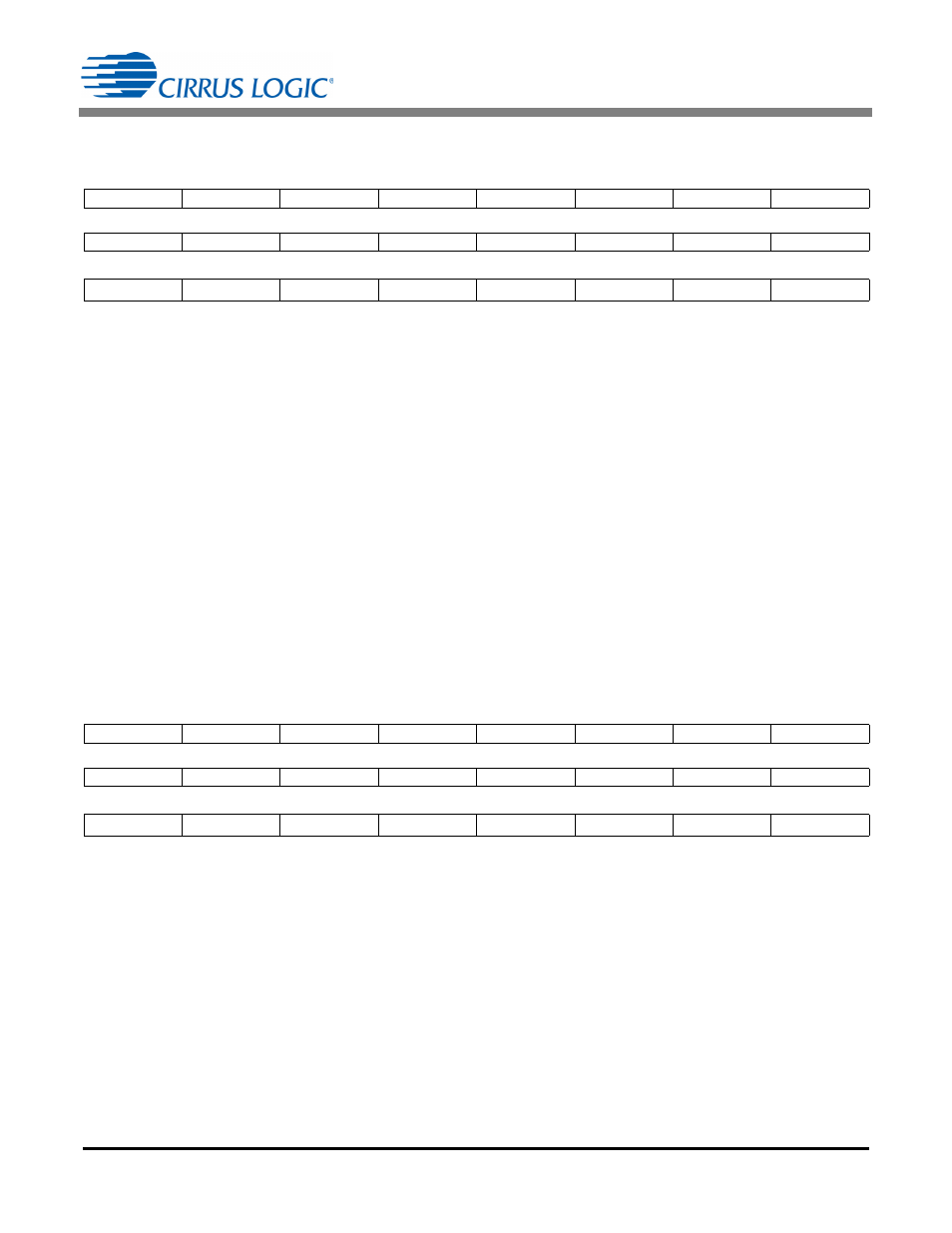
6.6.8 Pulse Output Control (PulseCtrl) – Page 0, Address 9
Default = 0x00 0000
This register controls the input to the energy pulse generation (EPG) block.
[23:4]
Reserved.
EPGIN[3:0]
Selects the input to the energy pulse generation (EPG) block.
0000 = P
AVG
(Default)
0001 = Reserved
0010 = P
SUM
0011 = Q
AVG
0100 = Reserved
0101 = Q
SUM
0110 = S
0111 = Reserved
1000 = S
SUM
1001 = Unused
...
1111 = Unused
6.6.9 Register Lock Control (RegLock) – Page 0, Address 34
Default = 0x00 0000
[23:13]
Reserved.
DSP_LCK[12:8] DSP_LCK[4:0] = 0x16 sets the DSP lockable registers to be write protected from the
CS5490 internal calculation engine. Writing 0x09 unlocks the registers.
[7:5]
Reserved.
HOST_LCK[4:0] HOST_LCK[4:0] = 0x16 sets all the registers except RegLock, Status0, Status1, and
Status2 to be write protected from the serial interface. Writing 0x09 unlocks the registers.
23
22
21
20
19
18
17
16
-
-
-
-
-
-
-
-
15
14
13
12
11
10
9
8
0
0
0
0
0
0
0
0
7
6
5
4
3
2
1
0
0
0
0
0
EPGIN[3]
EPGIN[2]
EPGIN[1]
EPGIN[0]
23
22
21
20
19
18
17
16
-
-
-
-
-
-
-
-
15
14
13
12
11
10
9
8
-
-
-
DSP_LCK[4]
DSP_LCK[3]
DSP_LCK[2]
DSP_LCK[1]
DSP_LCK[0]
7
6
5
4
3
2
1
0
-
-
-
HOST_LCK[4] HOST_LCK[3] HOST_LCK[2] HOST_LCK[1] HOST_LCK[0]
