Signal flow description, 1 analog-to-digital converters, 2 decimation filters – Cirrus Logic CS5490 User Manual
Page 15: 3 iir filter, 4 phase compensation, 5 dc offset & gain correction, Cs5490
CS5490
DS982F3
15
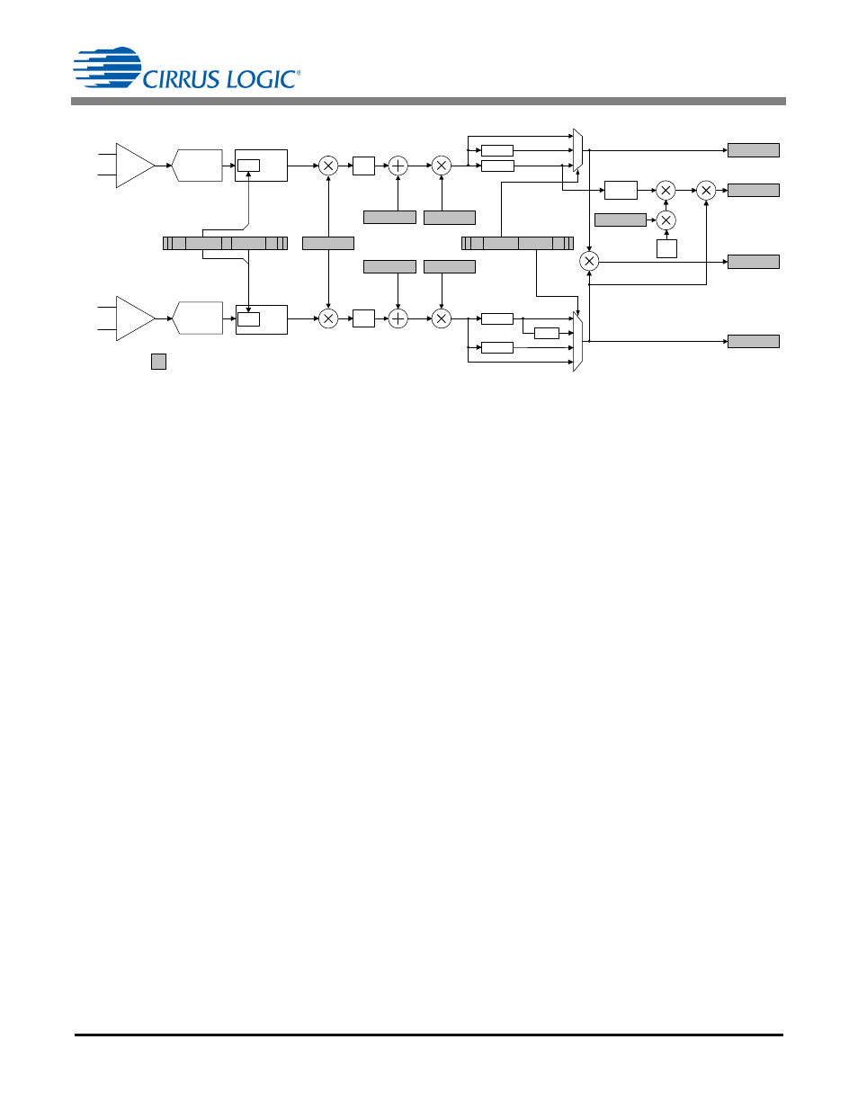
4. SIGNAL FLOW DESCRIPTION
The signal flow for voltage, current measurement, and
the other calculations is shown in
.
The signal flow consists of a current and a voltage
channel. The current and voltage channels have
differential input pins.
4.1 Analog-to-Digital Converters
Both input channels use fourth-order delta-sigma
modulators to convert the analog inputs to single-bit
digital data streams. The converters sample at a rate of
MCLK/8. This high sampling provides a wide dynamic
range and simplifies anti-alias filter design.
4.2 Decimation Filters
The single-bit modulator output data is widened to 24
bits and down sampled to MCLK/1024 with low-pass
decimation filters. These decimation filters are
third-order Sinc filters. The filter outputs pass through
an IIR "anti-sinc" filter.
4.3 IIR Filter
The IIR filter is used to compensate for the amplitude
roll-off of the decimation filters. The droop-correction
filter flattens the magnitude response of the channel out
to the Nyquist frequency, thus allowing for accurate
measurements of up to 2kHz (MCLK = 4.096MHz). By
default, the IIR filters are enabled. The IIR filters can be
bypassed by setting the IIR_OFF bit in the Config2
register.
4.4 Phase Compensation
Phase compensation changes the phase of voltage
relative to current by adding a delay in the decimation
filters. The amount of phase shift is set by the PC
register bits CPCC[1:0] and FPCC[8:0] for the current
channel. For the voltage channel, only bits CPCC[1:0]
affect the delay.
Fine phase compensation control bits, FPCC[8:0],
provide up to 1/OWR delay in the current channel.
Coarse phase compensation control bits, CPCC[1:0],
provide an additional 1/OWR delay in the current
channel or up to 2/OWR delay in the voltage channel.
Negative delay in the voltage channel can be
implemented by setting longer delay in the current
channel than the voltage channel. For a OWR of
4000Hz, the delay range is ±500µs, a phase shift of
±8.99° at 50Hz and ±10.79° at 60Hz. The step size is
0.008789° at 50Hz and 0.010547° at 60Hz. For more
information about phase compensation, see section
4.5 DC Offset & Gain Correction
The system and CS5490 inherently have component
tolerances, gain, and offset errors, which can be
removed using the gain and offset registers. Each
measurement channel has its own set of gain and offset
registers. For every instantaneous voltage and current
sample, the offset and gain values are used to correct
DC offset and gain errors in the channel (see section
on page 52 for more details).
MU
X
VIN±
SINC
3
IIN±
SINC
3
PGA
HPF
4
th
Order
ΔΣ
Modulator
4
th
Order
ΔΣ
Modulator
x10
DELAY
CTRL
2
MU
X
PMF
HPF
PMF
IIR
IIR
Phase
Shift
Config 2
Epsilon
DELAY
CTRL
INT
Registers
Q
V
P
I
SYS
GAIN
...
...
IFLT[1:0]
VFLT[1:0]
V
DCOFF
I
DCOFF
I
GAIN
V
GAIN
PC
...
...
FPCC[8:0]
CPCC[1:0]
...
Figure 6. Signal Flow for V, I, P, and Q Measurements