Pin descriptions – Cirrus Logic CS42L52 User Manual
Page 8
8
DS680F2
CS42L52
3/1/13
1. PIN DESCRIPTIONS
Pin Name
#
Pin Description
SDA
1
Serial Control Data (Input/Output) - SDA is a data I/O in I²C Mode.
SCL
2
Serial Control Port Clock (Input) - Serial clock for the serial control port.
AD0
3
Address Bit 0 (Input) - Chip address bit 0.
SPKR_OUTA+
SPKR_OUTA-
SPKR_OUTB+
SPKR_OUTB-
4
6
7
9
PWM Speaker Output (Output) - Full-bridge amplified PWM speaker outputs.
VP
5
8
Power for PWM Drivers (Input) - Power supply for the PWM output driver stages.
-VHPFILT
10
Inverting Charge Pump Filter Connection (Output) - Power supply from the inverting charge
pump that provides the negative rail for the headphone/line amplifiers.
FLYN
11
Charge Pump Cap Negative Node (Output) - Negative node for the inverting charge pump’s fly-
ing capacitor.
FLYP
12
Charge Pump Cap Positive Node (Output) - Positive node for the inverting charge pump’s flying
capacitor.
+VHP
13
Positive Analog Power for Headphone (Input) - Positive voltage rail and power for the internal
headphone amplifiers and inverting charge pump.
HP/LINE_OUTB, A
14,15 Headphone/Line Audio Output (Output) - Stereo headphone or line level analog outputs.
VA
16
Analog Power (Input) - Positive power for the internal analog section.
12
11
13
14
15
16
17
18
19
20
29
30
28
27
26
25
24
23
22
21
39
40
38
37
36
35
34
33
32
31
2
1
3
4
5
6
7
8
9
10
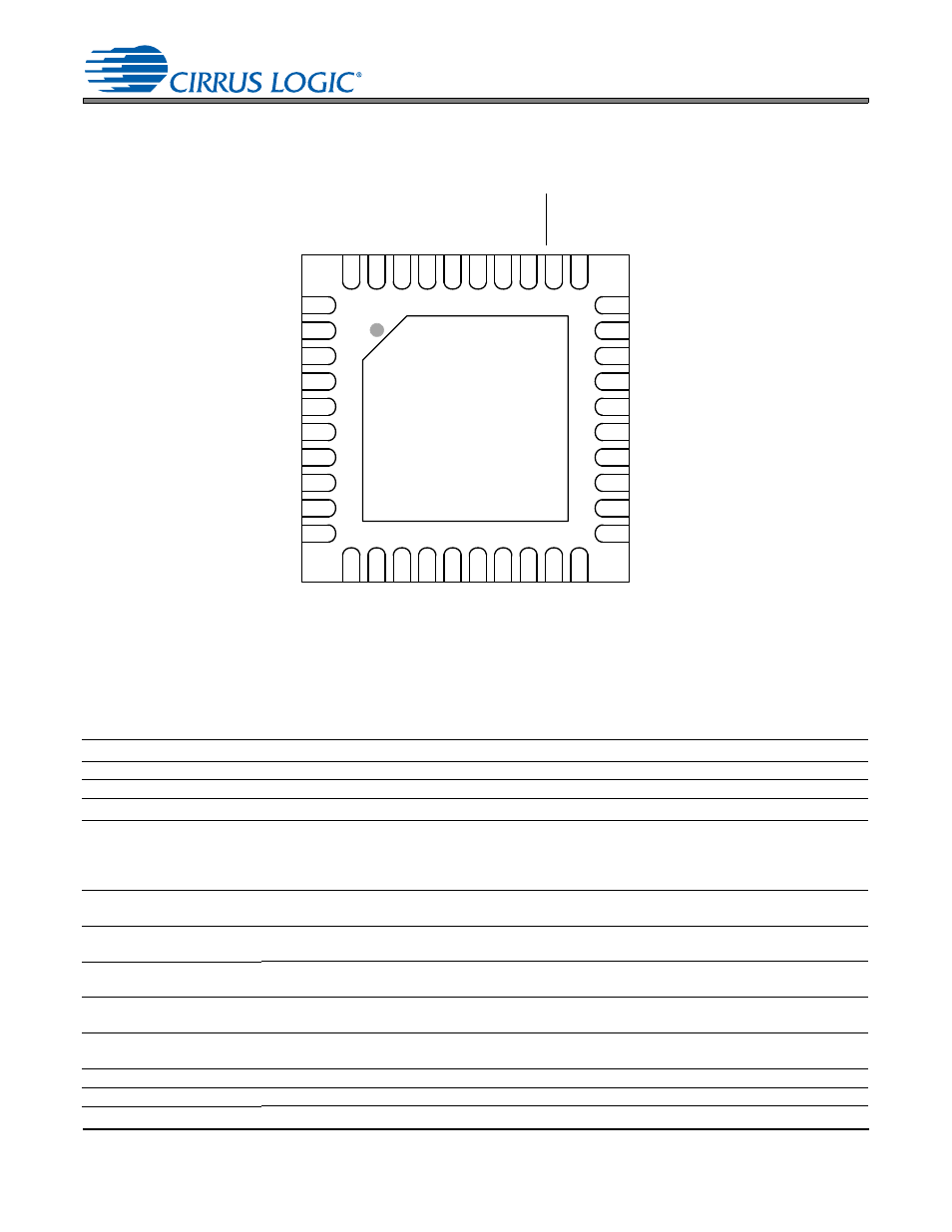
GND/Thermal Pad
SD
O
U
T
MCLK
SCLK
SDIN
SDA
LRC
K
FL
YN
+VHP
HP/L
INE_O
U
T
B
HP/L
INE_O
U
T
A
VQ
MICBIAS
AIN4A/MIC1+/MIC2A
AIN2A
AD0
SPKR_OUTA+
VP
VP
VD
SPKR_OUTB-
-VHPFILT
AIN4B/MIC2+/MIC2B
AIN1B
AIN2B
AFILTB
AIN3B/MIC2-/MIC1B
AFILTA
AIN1A
AIN3A/MIC1-/MIC1A
SPKR_OUTB+
SCL
DGND
SPKR_OUTA-
FL
YP
VA
AGND
FIL
T
+
R
ESET
VL
SPK
R/HP
Top-Down (Through-Package) View
40-Pin QFN Package