Cirrus Logic CS42L52 User Manual
Cs42l52, Stereo codec, Class d stereo/mono speaker amplifier
Copyright
Cirrus Logic, Inc. 2013
(All Rights Reserved)
MAR ’13
DS680F2
Low-Power, Stereo CODEC with Headphone and Speaker Amps
Stereo CODEC
High Performance Stereo ADC and DAC
–
99 dB (ADC), 98 dB (DAC) Dyn. Range (A-wtd)
–
-88 dB THD+N
Flexible Stereo Analog Input Architecture
–
4:1 Analog Input MUX
–
Analog Input Mixing
–
Analog Passthrough with Volume Control
–
Analog Programmable Gain Amplifier (PGA)
Programmable Automatic Level Control (ALC)
–
Noise Gate for Noise Suppression
–
Programmable Threshold and Attack/Release
Rates
Dual MIC Inputs
–
Differential or Single-ended
–
+16 dB to +32 dB with 1-dB step Mic Pre-
Amplifiers
–
Programmable, Low-noise MIC Bias Levels
Digital Signal Processing Engine
–
Bass and Treble Tone Control, De-emphasis
–
Master Vol. and Independent PCM SDIN + ADC
SDOUT Mix Volume Control
–
Soft-Ramp and Zero-Cross Transitions
–
Programmable Peak-detect and Limiter
–
Beep Generator w/Full Tone Control
Class D Stereo/Mono Speaker Amplifier
No External Filter Required
High-power Stereo Output at 10% THD+N
–
2 x 1.00 W into 8
@ 5.0 V
–
2 x 550 mW into 8
@ 3.7 V
–
2 x 230 mW into 8
@ 2.5 V
High-power Mono Output at 10% THD+N
–
1 x 1.90 W into 4
@ 5.0 V
–
1 x 1.00 W into 4
@ 3.7 V
–
1 x 350 mW into 4
@ 2.5 V
Direct Battery-powered Operation
–
Battery Level Monitoring and Compensation
81% Efficiency at 800 mW
Phase-aligned PWM Output Reduces Idle
Channel Current
Spread Spectrum Modulation
Low Quiescent Current
Stereo Headphone Amplifier
Ground-centered Outputs
–
No DC-Blocking Capacitors Required
–
Integrated Negative Voltage Regulator
High-power Output at -75 dB THD+N
–
2 x 23 mW Into 16
@ 1.8 V
–
2 x 44 mW Into 16
@ 2.5 V
)
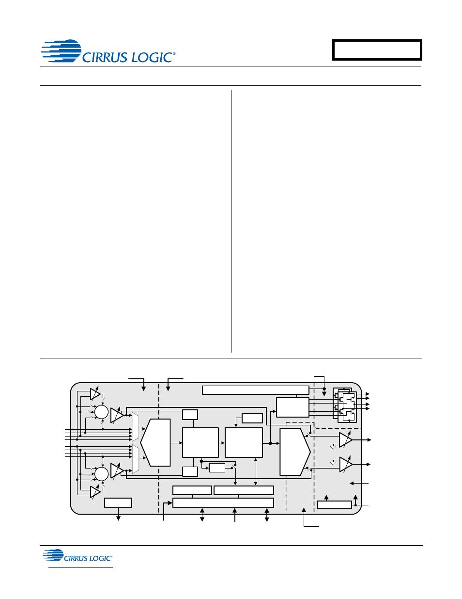
Serial Audio
Input/Output
I
2
C Control
+1.65 V to +3.47 V
Interface Supply
Control Port
Serial Audio Port
Level Shifter
Multi-bit
ADC
Beep
+1.65 V to +2.63 V
Analog Supply
Multi-bit
ADC
ALC
Left HP/Line
Output
Ground-Centered
Amps
Mono mix,
Limiter, Bass,
Treble Adjust
Volume, Mono
Swap, Mix
Right HP/Line
Output
Left
Inputs
Right
Inputs
+1.65 V to +2.63 V
Headphone Supply
Speaker/HP
Switch
+1.60 V to +5.25 V
Battery
Charge Pump
+VHP
-VHP
+1.65 V to +2.63 V
Digital Supply
+1.65 V to +2.63 V
Analog Supply
Pulse-Width
Modulator
(PWM)
Stereo/Mono
Full-Bridge
Speaker
Outputs
Battery Level Monitoring & Compensation
Multi-bit
DAC
MIC Bias
HPF
Selectable
Bias Voltage
ALC
Summing
Programmable
Gain Amps
+16 to +32 dB Diff./
S.E. MIC Pre-Amps
Class D Amps
1
2
3
4
1
2
3
4
+
-
+
-
Reset
CS42L52
DRAFTv1
3/1/13
Document Outline
- 1. Pin Descriptions
- 2. Typical Connection Diagram
- 3. Characteristic and Specifications
- Recommended Operating Conditions
- Absolute Maximum Ratings
- Analog Input Characteristics
- ADC Digital Filter Characteristics
- Analog Output Characteristics
- Analog Passthrough Characteristics
- PWM Output Characteristics
- Headphone Output Power Characteristics
- Line Output Voltage Level Characteristics
- Combined DAC Interpolation and onChip Analog FIlter Response
- Switching Specifications - Serial Port
- Switching Specifications - I²C Control Port
- DC Electrical Characteristics
- Digital Interface Specifications and Characteristics
- Power Consumption
- 4. Applications
- 4.1 Overview
- 4.2 Analog Inputs
- 4.3 Analog Outputs
- 4.4 Analog In to Analog Out Passthrough
- 4.5 PWM Outputs
- 4.6 Serial Port Clocking
- 4.7 Digital Interface Formats
- 4.8 Initialization
- 4.9 Recommended Power-up Sequence
- 4.10 Recommended Power-Down Sequence
- 4.11 Required Initialization Settings
- 4.12 Control Port Operation
- 5. Register Quick Reference
- 6. Register Description
- 6.1 Chip I.D. and Revision Register (Address 01h) (Read Only)
- 6.2 Power Control 1 (Address 02h)
- 6.3 Power Control 2 (Address 03h)
- 6.4 Power Control 3 (Address 04h)
- 6.5 Clocking Control (Address 05h)
- 6.6 Interface Control 1 (Address 06h)
- 6.7 Interface Control 2 (Address 07h)
- 6.8 Input x Select: ADCA and PGAA (Address 08h), ADCB and PGAB (Address 09h)
- 6.9 Analog and HPF Control (Address 0Ah)
- 6.10 ADC HPF Corner Frequency (Address 0Bh)
- 6.11 Misc. ADC Control (Address 0Ch)
- 6.12 Playback Control 1 (Address 0Dh)
- 6.13 Miscellaneous Controls (Address 0Eh)
- 6.14 Playback Control 2 (Address 0Fh)
- 6.15 MICx Amp Control:MIC A (Address 10h) and MIC B (Address 11h)
- 6.16 PGAx Vol. and ALCx Transition Ctl.: ALC, PGA A (Address 12h) and ALC, PGA B (Address 13h)
- 6.17 Passthrough x Volume: PASSAVOL (Address 14h) and PASSBVOL (Address 15h)
- 6.18 ADCx Volume Control: ADCAVOL (Address 16h) and ADCBVOL (Address 17h)
- 6.19 ADCx Mixer Volume: ADCA (Address 18h) and ADCB (Address 19h)
- 6.20 PCMx Mixer Volume: PCMA (Address 1Ah) and PCMB (Address 1Bh)
- 6.21 Beep Frequency and On Time (Address 1Ch)
- 6.22 Beep Volume and Off Time (Address 1Dh)
- 6.23 Beep and Tone Configuration (Address 1Eh)
- 6.24 Tone Control (Address 1Fh)
- 6.25 Master Volume Control: MSTA (Address 20h) and MSTB (Address 21h)
- 6.26 Headphone Volume Control: HPA (Address 22h) and HPB (Address 23h)
- 6.27 Speaker Volume Control: SPKA (Address 24h) and SPKB (Address 25h)
- 6.28 ADC and PCM Channel Mixer (Address 26h)
- 6.29 Limiter Control 1, Min/Max Thresholds (Address 27h)
- 6.30 Limiter Control 2, Release Rate (Address 28h)
- 6.31 Limiter Attack Rate (Address 29h)
- 6.32 ALC Enable and Attack Rate (Address 2Ah)
- 6.33 ALC Release Rate (Address 2Bh)
- 6.34 ALC Threshold (Address 2Ch)
- 6.35 Noise Gate Control (Address 2Dh)
- 6.36 Status (Address 2Eh) (Read Only)
- 6.37 Battery Compensation (Address 2Fh)
- 6.38 VP Battery Level (Address 30h) (Read Only)
- 6.39 Speaker Status (Address 31h) (Read Only)
- 6.40 Charge Pump Frequency (Address 34h)
- 7. Analog Performance Plots
- 8. Example System Clock Frequencies
- 9. PCB Layout Considerations
- 10. ADC and DAC Digital Filters
- 11. Parameter Definitions
- 12. Package Dimensions
- 13. Ordering Information
- 14. References
- 15. Revision History