Register description, 1 chip i.d. (read only), 2 chip revision (read only) – Cirrus Logic CS42L52 User Manual
Page 42: 2 power control 1 (address 02h), 1 power down adc charge pump, 2 power down pgax, 1 power down adc charge pump 6.2.2 power down pgax, Section 6, P 42
42
DS680F2
CS42L52
3/1/13
6. REGISTER DESCRIPTION
All registers are read/write except for the Chip I.D. and Revision Register and Interrupt Status Register, which are
read only. See the following bit definition tables for bit assignment information. The default state of each bit after a
power-up sequence or reset is listed in each bit description. Unless otherwise specified, all “Reserved” bits must
maintain their default value.
6.1
Chip I.D. and Revision Register (Address 01h) (Read Only)
6.1.1
Chip I.D. (Read Only)
I.D. code for the CS42L52.
6.1.2
Chip Revision (Read Only)
CS42L52 revision level.
6.2
Power Control 1 (Address 02h)
6.2.1
Power Down ADC Charge Pump
Configures the power state of the ADC charge pump.
6.2.2
Power Down PGAx
Configures the power state of PGA channel x.
Notes:
1.
The CS42L52 employs a scheme for controlling the power to the PGA when PASSTHRU (
) is enabled. Refer to the referenced application for more information.
2.
This bit should be used in conjunction with ADCxSEL and PGAxSEL bits to determine the analog
7
6
5
4
3
2
1
0
CHIPID4
CHIPID3
CHIPID2
CHIPID1
CHIPID0
REVID2
REVID1
REVID0
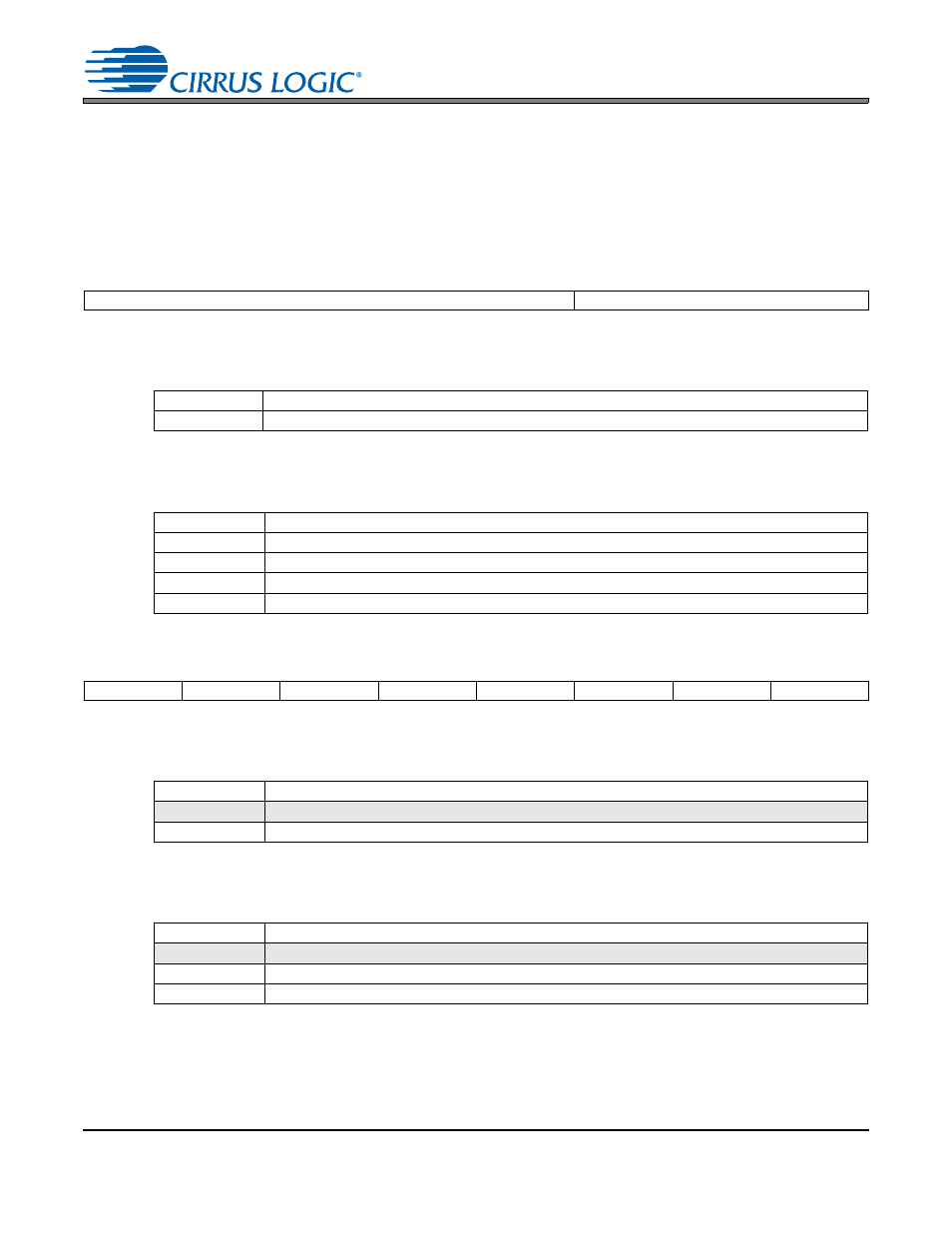
CHIPID[4:0]
Device
11100
CS42L52
REVID[2:0]
Revision Level
000
A0
001
A1
010
B0
011
B1
7
6
5
4
3
2
1
0
PDN_CHRG
Reserved
Reserved
PDN_PGAB
PDN_PGAA
PDN_ADCB
PDN_ADCA
PDN
PDN_CHRG
ADC Charge Pump Status
0
Powered Up
1
Powered Down
PDN_PGAx
PGA Status
0
Powered Up (ONLY when the ADC or the analog passthru is used)
1
Powered Down
Application