Applications information, Table 16. rom table – Rainbow Electronics MAX3540 User Manual
Page 12
MAX3540
Complete Single-Conversion Television Tuner
12
______________________________________________________________________________________
Applications Information
RF Inputs
The MAX3540 features separate UHF and VHF inputs
that are matched to 75Ω. Both inputs require a DC-block-
ing capacitor. The input registers select the active inputs.
In addition, the input registers enable or disable the low-
pass filter, which can be used when the VHF input is
selected. For 54MHz to 100MHz, select the VHF_IN with
the LPF filter enabled (INPT = 00). For 100MHz to
300MHz, select VHF_IN with LPF disabled (INPT = 01).
For 300MHz to 860MHz, select UHF_IN (INPT = 10).
RF Gain Control
The gain of the RF low-noise amplifier can be adjusted
over a typical 45dB range by the RFAGC pin. The
RFAGC input accepts a DC voltage from 0.5V to 3V,
with 3V providing maximum gain. This pin can be con-
trolled with the IF power-detector output to form a
closed RF gain-control loop. See the
Closed-Loop RF
Gain Control
section for more information.
RF Tracking Filter
The MAX3540 includes a programmable tracking filter for
each band of operation to optimize rejection of out-of-
band interference while minimizing insertion loss for the
desired received signal. VHF low, VHF high, or UHF track-
ing filter is selected by the TF register. The center fre-
quency of each tracking filter is selected by a switched-
capacitor array, which is programmed by the TFS[7:0]
bits in the Tracking-Filter Series Cap register and the
TFP[5:0] bits in the Tracking-Filter Parallel Cap register.
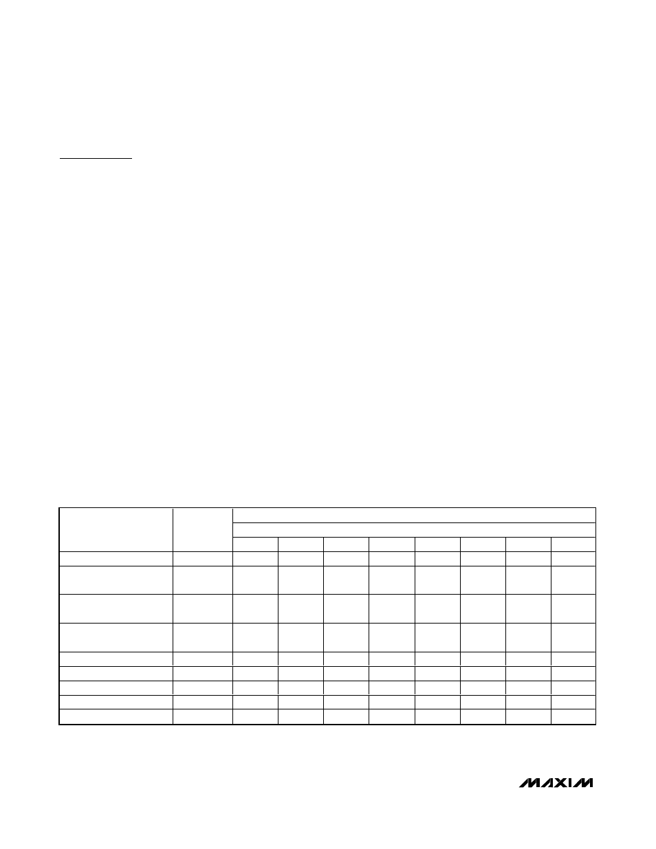
To accommodate part-to-part variations each part is fac-
tory-calibrated by Maxim. During calibration the y-inter-
cept and slope for the series and parallel tracking
capacitor arrays is calculated and written into an internal
ROM table. The user must read the ROM table upon
power-up and store the data in local memory (8 bytes
total) to calculate the optimal TFS[7:0] and TFP[5:0] set-
tings for each channel. Table 16 shows the address and
bits for each ROM table entry. See the
Interpolating
Tracking Filter Coefficients
section for more information
on how to calculate the required values.
Reading the ROM Table
Each ROM table entry must be read using a two-step
process. First, the address of the ROM bits to be read
must be programmed into the TFA[3:0] bits in the
Tracking Filter ROM Address register (Table 11).
Once the address has been programmed, the data
stored in that address is transferred to the TFR[7:0] bits
in the ROM Table Data Readback register (Table 13).
The ROM data at the specified address can then be
read from the TFR[7:0] bits and stored in the micro-
processor’s local memory.
MSB LSB
DATA BYTE
DESCRIPTION
ADDRESS
D7
D6
D5
D4
D3
D2
D1
D0
IFOVLD
0x0
OD2
OD1
OD0
X
X
X
X
X
VHF Low Series/
Parallel Y-Intercept
0x1
LS0[5]
LS0[4]
LS0[3]
LS0[2]
LS0[1]
LS0[0]
LS1[3]
LS1[2]
VHF High Series/
Parallel Y-Intercept
0x2
LS1[1]
LS1[0]
LP0[5]
LP0[4]
LP0[3]
LP0[2]
LP0[1]
LP0[0]
UHF Series/
Parallel Y-Intercept
0x3
LP1[3]
LP1[2]
LP1[1]
LP1[0]
HS0[3]
HS0[2]
HS0[1]
HS0[0]
VHF Low Series Slope
0x4
HS1[3]
HS1[2]
HS1[1]
HS1[0]
HP0[3]
HP0[2]
HP0[1]
HP0[0]
VHF High Parallel Slope
0x5
HP1[3]
HP1[2]
HP1[1]
HP1[0]
US0[7]
US0[6]
US0[5]
US0[4]
VHF Low Parallel Slope
0x6
US0[3]
US0[2]
US0[1]
US0[0]
US1[5]
US1[4]
US1[3]
US1[2]
VHF High Parallel Slope
0x7
US1[1]
US1[0]
UP0[7]
UP0[6]
UP0[5]
UP0[4]
UP0[3]
UP0[2]
UHF Parallel Slope
0x8
UP0[1]
UP0[0]
UP1[5]
UP1[4]
UP1[3]
UP1[2]
UP1[1]
UP1[0]
Table 16. ROM Table