Rainbow Electronics MAX3540 User Manual
Page 11
MAX3540
Complete Single-Conversion Television Tuner
______________________________________________________________________________________
11
The MAX3540 continuously awaits a START condition
followed by its slave address. When the device recog-
nizes its slave address, it acknowledges by pulling the
SDA line low for one clock period. It is ready to accept
or send data depending on the R/
W bit (Figure 1).
Write Cycle
When addressed with a write command, the MAX3540
allows the master to write to a single register or to multi-
ple successive registers.
A write cycle begins with the bus master issuing a
START condition followed by the 7 slave address bits
and a write bit (R/
W = 0). The MAX3540 issues an ACK
if the slave address byte is successfully received. The
bus master must then send to the slave the address of
the first register it wishes to write to. If the slave
acknowledges the address, the master can then write
one byte to the register at the specified address. Data
is written beginning with the most significant bit. The
MAX3540 again issues an ACK if the data is success-
fully written to the register. The master can continue to
write data to the successive internal registers with the
MAX3540 acknowledging each successful transfer, or it
can terminate transmission by issuing a STOP condi-
tion. The write cycle does not terminate until the master
issues a STOP condition.
Figure 2 illustrates an example in which registers 0
through 2 are written with 0x0E, 0xD8, and 0xE1,
respectively.
Read Cycle
A read cycle begins with the bus master issuing a
START condition followed by the seven slave address
bits and a write bit (R/
W = 0). The MAX3540 issues an
ACK if the slave address byte is successfully received.
The master then sends the 8-bit address of the first reg-
ister that it wishes to read. The MAX3540 then issues
another ACK. Next, the master must issue a START con-
dition followed by the 7 slave address bits and a read
bit (R/
W = 1). The MAX3540 issues an ACK if it success-
fully recognizes its address and begins sending data
from the specified register address starting with the
most significant bit (MSB). Data is clocked out of the
MAX3540 on the rising edge of SCL. On the 9th rising
edge of SCL, the master can issue an ACK and contin-
ue reading successive registers or it can issue a NACK
followed by a STOP condition to terminate transmission.
The read cycle does not terminate until the master
issues a STOP condition. Figure 3 illustrates an example
in which registers 0 and 1 are read back.
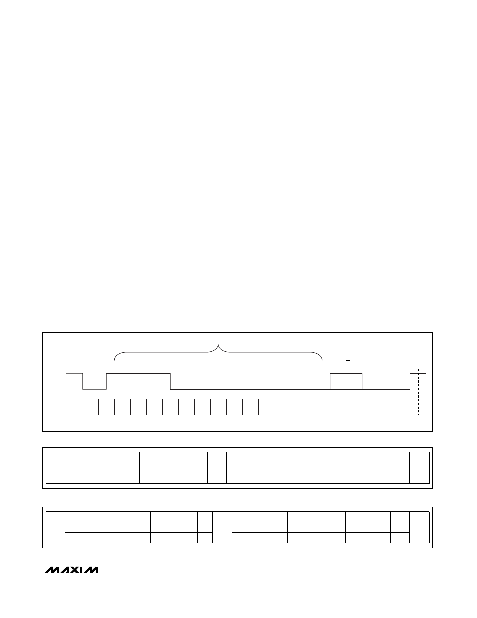
SCL
SDA
1
2
3
4
5
6
7
8
9
S
1
1
0
0
0
ADDR2
ADDR1
R/W
ACK
SLAVE ADDRESS
P
NOTE: TIMING PARAMETERS CONFORM WITH I
2
C BUS SPECIFICATIONS.
Figure 1. MAX3540 Slave Address Byte
WRITE DEVICE
ADDRESS
R/W
ACK
WRITE REGISTER
ADDRESS
ACK
WRITE DATA TO
REGISTER 0x00
ACK
WRITE DATA TO
REGISTER 0x01
ACK
WRITE DATA TO
REGISTER 0x02
ACK
START
11000[ADDR2][ADDR1]
0
—
0x00
—
0x0E
—
0xD8
—
0xE1
—
STOP
Figure 2. Example: Write registers 0 through 2 with 0x0E, 0xD8, and 0xE1, respectively.
WRITE DEVICE
ADDRESS
R/W
ACK
WRITE 1st REGISTER
ADDRESS
ACK
WRITE DEVICE
ADDRESS
R/W
ACK
READ DATA
REG 0
ACK
READ DATA
REG 1
NACK
START
110000[ADDR2][ADDR1]
0
—
0x00
—
START
110000[ADDR2][ADDR1]
1
—
D7–D0
—
D7–D0
—
STOP
Figure 3. Example: Read data from registers 0 through 1.