Rainbow Electronics MAX3540 User Manual
Page 10
MAX3540
Complete Single-Conversion Television Tuner
10
______________________________________________________________________________________
2-Wire Serial Interface
The MAX3540 uses a 2-wire I
2
C-compatible serial inter-
face consisting of a serial-data line (SDA) and a serial-
clock line (SCL). SDA and SCL facilitate bidirectional
communication between the MAX3540 and the master at
clock frequencies up to 400kHz. The master initiates a
data transfer on the bus and generates the SCL signal to
permit data transfer. The MAX3540 behaves as a slave
device that transfers and receives data to and from the
master. Pull SDA and SCL high with external pullup
resistors (1kΩ or greater) for proper bus operation.
One bit is transferred during each SCL clock cycle. A
minimum of nine clock cycles is required to transfer a
byte in or out of the MAX3540 (8 data bits and an
ACK/NACK). The data on SDA must remain stable during
the high period of the SCL clock pulse. Changes in SDA
while SCL is high and stable are considered control sig-
nals (see the
START and STOP Conditions
section). Both
SDA and SCL remain high when the bus is not busy.
START and STOP Conditions
The master initiates a transmission with a START condi-
tion (S), which is a high-to-low transition on SDA while
SCL is high. The master terminates a transmission with
a STOP condition (P), which is a low-to-high transition
on SDA while SCL is high.
Acknowledge and Not-Acknowledge Conditions
Data transfers are framed with an acknowledge bit
(ACK) or a not-acknowledge bit (NACK). Both the mas-
ter and the MAX3540 (slave) generate acknowledge
bits. To generate an acknowledge, the receiving device
must pull SDA low before the rising edge of the
acknowledge-related clock pulse (ninth pulse) and
keep it low during the high period of the clock pulse.
To generate a not-acknowledge condition, the receiver
allows SDA to be pulled high before the rising edge of
the acknowledge-related clock pulse, and leaves SDA
high during the high period of the clock pulse. Monitoring
the acknowledge bits allows for detection of unsuccessful
data transfers. An unsuccessful data transfer happens
if a receiving device is busy or if a system fault has
occurred. In the event of an unsuccessful data transfer,
the bus master must reattempt communication at a
later time.
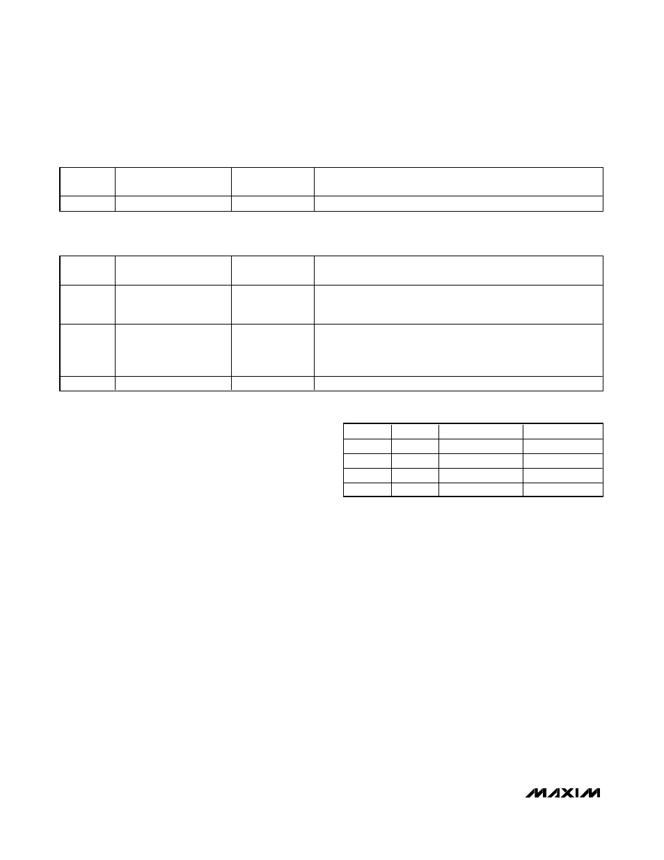
Slave Address
The MAX3540 has a 7-bit slave address that must be
sent to the device following a START condition to initi-
ate communication. The slave address is determined
by the state of the ADDR2 and ADDR1 pins and is
equal to 11000[ADDR2][ADDR1]. The 8th bit (R/
W) fol-
lowing the 7-bit address determines whether a read or
write operation will occur. Table 15 shows the possible
address configurations.
BIT NAME
BIT LOCATION (0 = LSB)
RECOMMENDED
DEFAULT
FUNCTION
TFR[7:0]
7–0
00000000*
Tracking-filter data bits read from the device’s ROM table.
Table 13. ROM Table Data Readback Register (Address: 1011
b
)
BIT NAME
BIT LOCATION (0 = LSB)
RECOMMENDED
DEFAULT
FUNCTION
POR
7
0
Power-on reset.
0 = status register has been read
1 = power reset since last status register read
LD[2:0]
6, 5, 4
000
VCO tuning voltage indicators.
000 = PLL not in lock, tune to the next lowest sub-band
001–110 = PLL in lock
111 = PLL not in lock, tune to the next higher sub-band
Reserved
3–0
0000
Reserved.
Table 14. Status Register (Address: 1100
b
)
ADDR2
ADDR1
WRITE ADDRESS
READ ADDRESS
0
0
0xC0
0xC1
0
1
0xC2
0xC3
1
0
0xC4
0xC5
1
1
0xC6
0xC7
Table 15. MAX3540 Address Configurations
*
See the RF Tracking Filter section.