Ds1841 temperature-controlled, nv, i, C, logarithmic resistor – Rainbow Electronics DS1841 User Manual
Page 9
DS1841
Temperature-Controlled, NV, I
2
C,
Logarithmic Resistor
_______________________________________________________________________________________
9
Supply Voltage Monitoring
The DS1841 also features an internal 8-bit supply volt-
age (V
CC
) monitor. A value of the supply voltage mea-
surement can be read over I
2
C at the address 0Eh.
To calculate the supply voltage, simply convert the
hexadecimal result into decimal and then multiply it by
the LSB as shown in
the Analog Voltage Monitoring
Characteristics
electrical table.
Supply Current (I
CC
)
The DS1841 has two supply current levels of power sup-
ply consumption. First, active current during I
2
C com-
munications while in the LUT-Driven Mode is the “worst
case” supply current, I
CC
. All functionality including I
2
C
communication is operating simultaneously. Second,
active current without I
2
C while in the LUT-Driven Mode
is quantified by the supply current, I
CC2
. SDA and SCL
are held statically in the high logic level.
Slave Address Byte and Address Pins
The slave address byte consists of a 7-bit slave
address plus a R/W bit (see Figure 2). The DS1841’s
slave address is determined by the state of the A0 and
A1 address pins. These pins allow up to four devices to
reside on the same I
2
C bus. Address pins tied to GND
result in a 0 in the corresponding bit position in the
slave address. Conversely, address pins tied to V
CC
result in a 1 in the corresponding bit positions. For
example, the DS1841’s slave address byte is 50h when
A0 and A1 pins are grounded. I
2
C communication is
described in detail in the
I
2
C Serial Interface
Description
section.
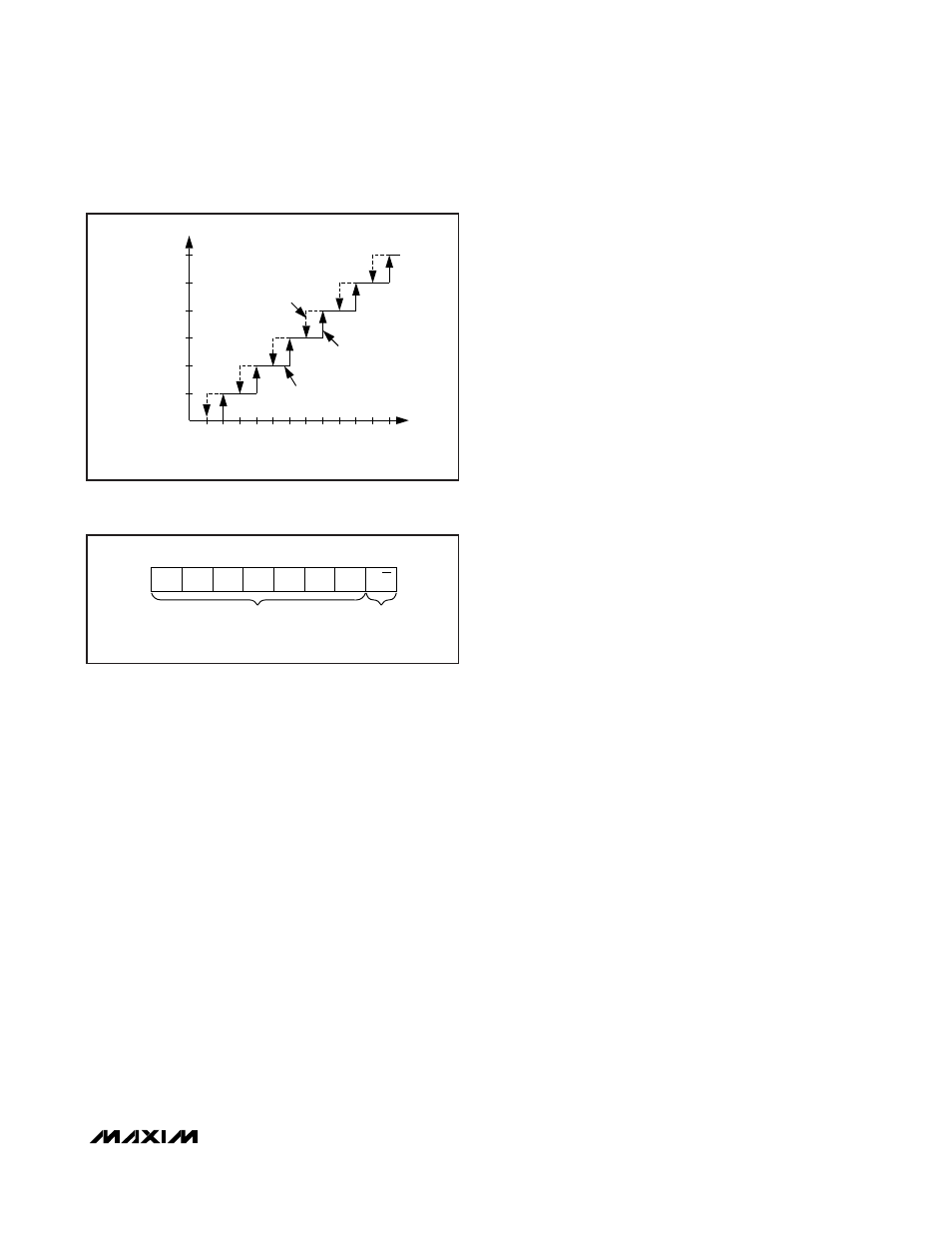
MEMORY LOCATION
TEMPERATURE (
°C)
LUT34
DECREASING
TEMPERATURE
INCREASING
TEMPERATURE
1
°C HYSTERESIS
WINDOW
LUT33
LUT32
LUT31
LUT30
19
21
23
25
19
27
Figure 1. LUT Hysteresis
0
1
1
0
R/W
A0
A1
0
MSB
LSB
READ/WRITE BIT
SLAVE ADDRESS*
*THE SLAVE ADDRESS IS DETERMINED BY ADDRESS PINS A0, A1.
Figure 2. Slave Address Byte