Ds1841 temperature-controlled, nv, i, C, logarithmic resistor – Rainbow Electronics DS1841 User Manual
Page 14
DS1841
Temperature-Controlled, NV, I
2
C,
Logarithmic Resistor
14
______________________________________________________________________________________
Byte read: A byte read is an 8-bit information transfer
from the slave to the master plus a 1-bit ACK or NACK
from the master to the slave. The 8 bits of information
that are transferred (most significant bit first) from the
slave to the master are read by the master using the bit
read definition, and the master transmits an ACK using
the bit write definition to receive additional data bytes.
The master must NACK the last byte read to terminate
communication so the slave returns control of SDA to
the master.
Slave address byte: Each slave on the I
2
C bus
responds to a slave address byte sent immediately fol-
lowing a START condition. The slave address byte con-
tains the slave address in the most significant 7 bits
and the R/W bit in the least significant bit.
The DS1841’s slave address is determined by the state
of the A0 and A1 address pins as shown in Figure 2.
Address pins tied to GND result in a 0 in the corre-
sponding bit position in the slave address. Conversely,
address pins tied to V
CC
result in a 1 in the corre-
sponding bit positions.
When the R/W bit is 0 (such as in 50h), the master is
indicating that it will write data to the slave. If R/W = 1
(51h in this case), the master is indicating that it wants
to read from the slave.
If an incorrect slave address is written, the DS1841
assumes the master is communicating with another I
2
C
device and ignores the communication until the next
START condition is sent.
Memory address: During an I
2
C write operation, the
master must transmit a memory address to identify the
memory location where the slave is to store the data.
The memory address is always the second byte trans-
mitted during a write operation following the slave
address byte.
I
2
C Communication
Writing a single byte to a slave: The master must gen-
erate a START condition, write the slave address byte
(R/W = 0), write the memory address, write the byte of
data, and generate a STOP condition. Remember the
master must read the slave’s acknowledgment during
all byte write operations.
When writing to the DS1841, the potentiometer adjusts to
the new setting once it has acknowledged the new data
that is being written, and the EEPROM is written following
the STOP condition at the end of the write command. To
change the setting without changing the EEPROM, termi-
nate the write with a repeated START condition before
the next STOP condition occurs. Using a repeated
START condition prevents the t
W
delay required for the
EEPROM write cycle to finish.
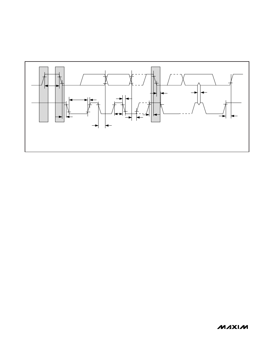
SDA
SCL
t
HD:STA
t
LOW
t
HIGH
t
R
t
F
t
BUF
t
HD:DAT
t
SU:DAT
REPEATED
START
t
SU:STA
t
HD:STA
t
SU:STO
t
SP
STOP
NOTE: TIMING IS REFERENCE TO V
IL(MAX)
AND V
IH(MIN)
.
START
Figure 3. I2C Timing Diagram