Ds1841 temperature-controlled, nv, i, C, logarithmic resistor, Applications information – Rainbow Electronics DS1841 User Manual
Page 16: Package information, Appendix a: control bits logic table
DS1841
Temperature-Controlled, NV, I
2
C,
Logarithmic Resistor
Maxim cannot assume responsibility for use of any circuitry other than circuitry entirely embodied in a Maxim product. No circuit patent licenses are
implied. Maxim reserves the right to change the circuitry and specifications without notice at any time.
16 ____________________Maxim Integrated Products, 120 San Gabriel Drive, Sunnyvale, CA 94086 408-737-7600
© 2007 Maxim Integrated Products
is a registered trademark of Maxim Integrated Products, Inc.
tion, writes the slave address byte (R/W = 1), reads
data with ACK or NACK as applicable, and generates a
STOP condition. See Figure 4 for I
2
C Communication
Examples.
Applications Information
Power-Supply Decoupling
To achieve the best results when using the DS1841,
decouple both the power-supply pin and the wiper-bias
voltage pin with a 0.01µF or 0.1µF capacitor. Use a
high-quality ceramic surface-mount capacitor if possi-
ble. Surface-mount components minimize lead induc-
tance, which improves performance, and ceramic
capacitors tend to have adequate high-frequency
response for decoupling applications.
SDA and SCL Pullup Resistors
SDA is an I/O with an open-collector output that
requires a pullup resistor to realize high-logic levels. A
master using either an open-collector output with a
pullup resistor or a push-pull output driver can be used
for SCL. Pullup resistor values should be chosen to
ensure that the rise and fall times listed in the AC elec-
trical characteristics are within specification. A typical
value for the pullup resistors is 4.7k
Ω.
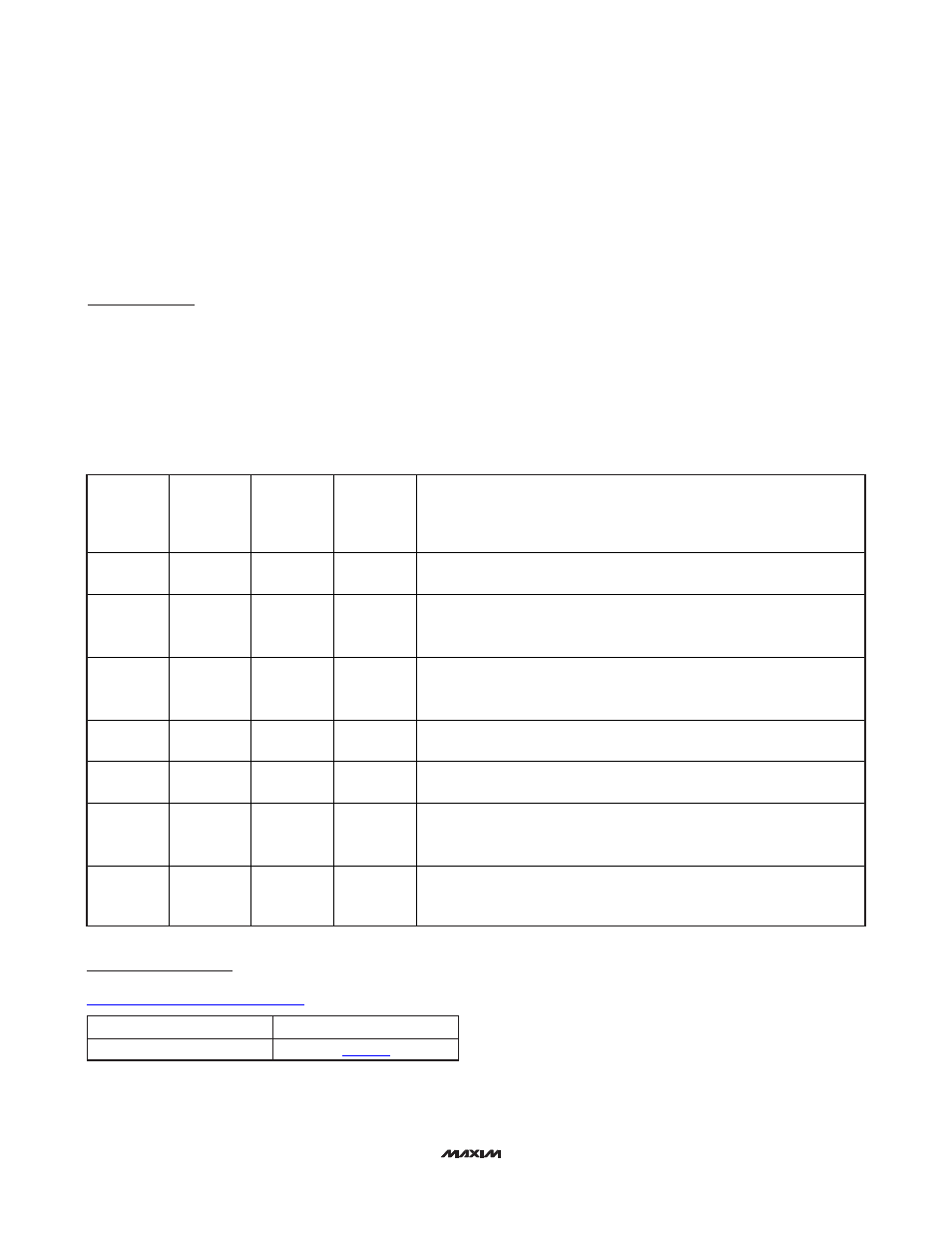
Appendix A: Control Bits Logic Table
LUTAR
MODE BIT
WIPER
ACCESS
CONTROL
BIT
ADDER
MODE BIT
UPDATE
MODE BIT
CONTROL OF WR AND REGISTER FUNCTIONALITY
X X X 0
IVR is loaded to WR on power-up. Subsequent writes to 00h set the value
of WR.
0 0 0 1
Temperature conversion references the LUT, determining LUTAR value,
the LUTAR determines the LUTVAL value, the unsigned LUTVAL value
is then automatically loaded into WR.
0 0 1 1
Temperature conversion references the LUT, determining LUTAR value,
the LUTAR sets the LUTVAL value, the signed LUTVAL value is then
summed with IVR, and the result is loaded into WR.
X 1 0 1
I
2
C Write (to 09h): The unsigned value written to WR, register 09h, is
loaded into WR.
X 1 1 1
I
2
C Write (to 09h): The signed value of LUTVAL is summed with IVR, then
loaded into WR, register 09h.
1 0 0 1
I
2
C Write (to 08h): LUTAR references LUT address, value at LUT address
location is loaded into LUTVAL, the unsigned LUTVAL value is loaded
into WR.
1 0 1 1
I
2
C Write (to 08h): LUTAR references LUT address, the signed value at
LUT address location is loaded into LUTVAL, the signed LUTVAL value
is summed with IVR value, and the result is loaded into WR.
Package Information
(For the latest package outline information, go to
www.maxim-ic.com/DallasPackInfo
.)
PACKAGE TYPE
DOCUMENT NO.
10 TDFN