Silicon Laboratories SI2493/57/34/15/04 User Manual
A n 9 3, Introduction, Figure 1. functional block diagram
Rev. 1.3 8/11
Copyright © 2011 by Silicon Laboratories
AN93
This information applies to a product under development. Its characteristics and specifications are subject to change without notice.
A N 9 3
S i 2 4 9 3 / 5 7 / 3 4 / 1 5 / 0 4 ( R e v i s i o n D ) a n d S i 2 4 9 4 / 3 9
M o d e m D e s i g n e r ’s G u i d e
1. Introduction
The Si2494/93/57/39/34/15/04 ISOmodem chipset family consists of a 38-pin QFN (Si2494/39) or 24-pin TSSOP
(Si2493/57/34/15/04) or 16-pin SOIC (Si2493/57/34/15/04) low-voltage modem device, and a 16-pin SOIC line-
side DAA device (Si3018/10) connecting directly with the telephone local loop (Tip and Ring). This modem solution
is a complete hardware (controller-based) modem that connects to a host processor through a UART, parallel or
SPI interface. Parallel and EEPROM interfaces are available only on the 38-pin QFN or 24-pin TSSOP package
option. Refer to Table 4, “ISOmodem Capabilities,” on page 10 for available part number, capability and package
combinations. Isolation is provided by Silicon Laboratories’ isolation capacitor technology, which uses high-voltage
capacitors instead of a transformer. This isolation technology complies with global telecommunications standards
including FCC, ETSI ES 203 021, JATE, and all known country-specific requirements.
Additional features include programmable ac/dc termination and ring impedance, on-hook and off-hook intrusion
detection, Caller ID, loop voltage/loop current monitoring, overcurrent detection, ring detection, and the hook-
switch function. All required program and data memory is included in the modem device. When the modem
receives a software or hardware reset, all register settings revert to the default values stored in the on-chip
program memory. The host processor interacts with the modem controller through AT commands used to change
register settings and control modem operation. Country, EMI/EMC, and safety test reports are available from
Silicon Laboratories representatives and distributors.
This application note is intended to supplement the Si2494/39 Revision A, Si2493 Revision D, and the Si2457/34/
15/04 Revision D data sheets. It provides all the hardware and software information necessary to implement a
variety of modem applications, including reference schematics, sample PCB layouts, AT command and register
reference, country configuration tables, programming examples and more. Particular topics of interest can be
easily located through the table of contents or the comprehensive index located at the back of this document.
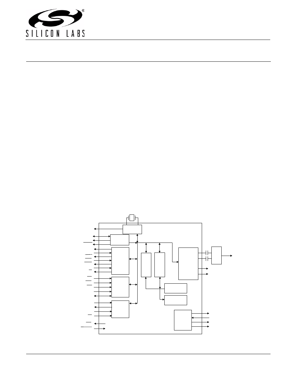
Figure 1. Functional Block Diagram
UART
Interface
Parallel
Interface
DSP
DAA
Interface
ROM
PLL
Clocking
XTI
XTO
CLKOUT
INT
RESET
C1
To Phone
Line
AOUT
Data Bus
Cont
rol
ler
Si
3018
/1
0
RXD
TXD
CTS
RTS
DCD
ESC
RI
CS
WR
RD
A0
D0-D7
Program Bus
RAM
EEPROM
Interface
EESD
EECLK
EECS
C2
Si3000
Interface
FSYNC
SDO
SDI
MCLK
SPI
Interface
SDI
SDO
SCLK
SS
AOUTb
Document Outline
- 1. Introduction
- 2. Modem (System-Side) Device
- 3. DAA (Line-Side) Device
- 4. Hardware Design Reference
- 5. Modem Reference Guide
- 5.1. Controller
- 5.2. DSP
- 5.3. Memory
- 5.4. AT Command Set
- 5.5. Extended AT Commands
- 5.6. S Registers
- 5.7. U Registers
- 5.7.1. U-Register Summary
- 5.7.2. U00–U16 (Dial Tone Detect Filter Registers)
- 5.7.3. U17–U30 (Busy Tone Detect Filter Registers)
- 5.7.4. U31–U33 (Ringback Cadence Registers)
- 5.7.5. U34–U35 (Dial Tone Timing Register)
- 5.7.6. U37–U45 (Pulse Dial Registers)
- 5.7.7. U46–U48 (DTMF Dial Registers)
- 5.7.8. U49–U4C (Ring Detect Registers)
- 5.7.9. U4D (Modem Control Register 1—MOD1)
- 5.7.10. U4E (Pre-Dial Delay Time Register)
- 5.7.11. U4F (Flash Hook Time Register)
- 5.7.12. U50–U51 (Loop Current Debouncing Registers)
- 5.7.13. U52 (Transmit Level Register)
- 5.7.14. U53 (Modem Control Register 2)
- 5.7.15. U54 (Calibration Timing Register)
- 5.7.16. U62–U66 (DAA Control Registers)
- 5.7.17. U67–U6A (International Configuration Registers)
- 5.7.18. U6C (Line-Voltage Status Register)
- 5.7.19. U6E–U7D (Modem Control and Interface Registers)
- 5.7.20. U80 (Transmit Delay for V.22 Fast Connect)
- 5.7.21. U87 (Synchronous Access Mode Configuration Register)
- 5.7.22. UAA (V.29 Mode Register)
- 5.7.23. UIDA Response and Answer Tone Delay Register
- 5.8. Firmware Upgrades
- 5.9. Escape Methods
- 5.10. Data Compression
- 5.11. Error Correction
- 5.12. Wire Mode
- 5.13. EPOS (Electronic Point of Sale) Applications
- 5.14. Legacy Synchronous DCE Mode/V.80 Synchronous Access Mode
- 5.15. V.80 Mode
- 6. Programming Examples
- 6.1. Quick Reference
- 6.2. Country-Dependent Setup
- 6.3. Caller ID
- 6.4. SMS Support
- 6.5. Type II Caller ID/SAS Detection
- 6.6. Intrusion/Parallel Phone Detection
- 6.7. Modem-On-Hold
- 6.8. HDLC: Bit Errors on a Noisy Line
- 6.9. Overcurrent Detection
- 6.10. Pulse/Tone Dial Decision
- 6.11. Telephone Voting Mode
- 6.12. V.92 Quick Connect
- 7. Handset, TAM, and Speakerphone Operation
- 7.1. Software Reference
- 7.2. Voice Reference—Overview
- 7.3. Si3000 Configuration
- 7.4. Initialization
- 7.5. Handset
- 7.6. Telephone Answering Machine
- 7.7. Speakerphone
- 7.7.1. Overview
- 7.7.2. Simplex Speakerphone
- 7.7.3. External Microphone/Speaker Calibration
- 7.7.4. Speakerphone Configuration
- 7.7.5. Simplex Speakerphone Configuration
- 7.7.6. Call—Automatic Tone Dial
- 7.7.7. Call—Manual Off-Hook Tone Dial
- 7.7.8. Call—Automatic Pulse Dial
- 7.7.9. Answer
- 7.7.10. Handset Transition
- 7.7.11. Termination
- 7.8. Glossary
- 7.9. References
- 8. Security Protocols
- 9. Chinese ePOS SMS
- 10. Testing and Diagnostics
- Appendix A—EPOS Applications
- Appendix B—Line Audio Recording
- Appendix C—Parallel/SPI Interface Software Implementation
- Document Change List
- Contact Information