Isomodem layout check list, An93, Figure 21. illustrated layout guidelines – Silicon Laboratories SI2493/57/34/15/04 User Manual
Page 51: Table 34. layout checklist, Rev. 1.3 51
AN93
Rev. 1.3
51
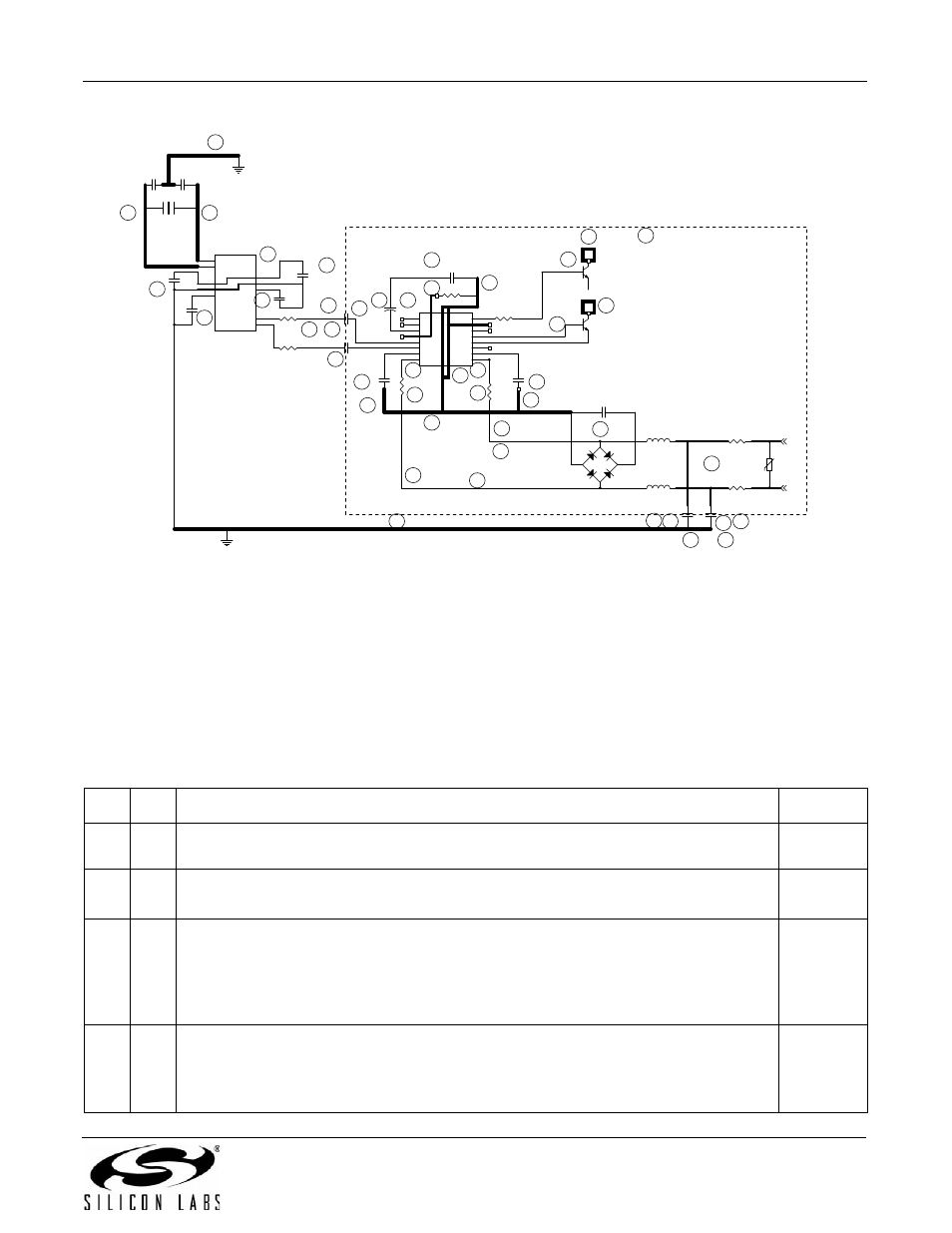
Figure 21. Illustrated Layout Guidelines
4.4.1. ISOmodem Layout Check List
Table 34 is a checklist that the designer can use during the layout process to ensure that all the recommendations
in this application note have been implemented. Additionally, Figure 21 provides an annotated diagram of all
relevant layout guidelines for the SI3054 CNR/AMR/ACR applications. See "10.4.2. Safety" on page 254 for
information about design for safety compliance.
Table 34. Layout Checklist
P
#
Layout Items
Required
1
U1 and U2 are placed so that pins 9–16 of U1 are facing pins 1–8 of U2. C1 and C2
are placed directly between U1 and U2.
2
Place U1, U2, C1, and C2 so that the recommended minimum creepage spacing for
the target application is implemented. R12 and R13 should be close to U1.
3
C1 and C2 should be placed directly between U1 and U2. Short, direct traces should
be used to connect C1 and C2 to U1 and U2. These traces should not be longer than
two inches and should be minimized in length. Place C2 such that its accompanying
trace to the C2B pin (pin 6) on the Si3018 is not close to the trace from R7 to the
RNG1 pin on the Si3018 (pin 8).
4
Place R7 and R8 as close as possible to the RNG1 and RNG2 pins (pins 8 and 9),
ensuring a minimum trace length from the RNG1 or RNG2 pin to the R7 or R8 resistor.
In order to space the R7 component further from the trace from C2 to the C2B pin, it is
acceptable to orient it 90 degrees relative to the RNG1 pin (pin 8).
RING
TIP
4A
4B
4C
4D
4E
4F
4G
4F
5
6
3A
3C 3E
3B
3A
3E
3E
3E
3E
7A
7B
7C
7C 7B
7B
9A
10
10
11
12
12
12
12
11
8C
8D
8D
9B
9C
9C
9C
11
2
2
2
2
This is not a complete schematic. Only critical component placement and nets are drawn.
1
Traces, pad sites and vias
enclosed in box are in the DAA
section, and must be separated
from all other circuits by 5 mm.
Note: Encircled references are described in the numbered paragraphs in Appendix A.
R9
R8
C9
FB2
C26
RV1
R12*
-
+
D1
R7
R16
C1
C5
C8
C50
Y1
1
2
U1 Si24HS
XTALI
1
XTALO
2
VDD3.3
5
GND
6
C1A
14
C1B
13
VDDA
7
VDD3.3
21
GND
20
VDDB
19
U2
Si3018
QE
1
DCT
2
RX
3
IB
4
C1B
5
C2B
6
VREG
7
RNG1
8
DCT2
16
IGND
15
DCT3
14
QB
13
QE2
12
SC
11
VREG2
10
RNG2
9
C53
R15
C52
C27
Q5
R2
C2
C7
Q4
+
C4
C6
FB1
C51
R13*
C3
*Note: Do NOT use ferrite
beads in place of R12 and
R13.