Silicon Laboratories SI5351A/B/C User Manual
S i 5 3 5 1 a / b / c, C - p, V c x o

Preliminary Rev. 0.95 8/11
Copyright © 2011 by Silicon Laboratories
Si5351A/B/C
This information applies to a product under development. Its characteristics and specifications are subject to change without notice.
S i 5 3 5 1 A / B / C
I
2
C - P
R O G R A M M A B L E
A
N Y
- F
R E Q U E N C Y
C M O S C
L O C K
G
E N E R A T O R
+ V C X O
Features
Applications
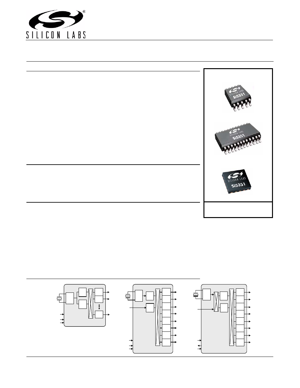
Description
The Si5351 is an I
2
C configurable clock generator that is ideally suited for replacing
crystals, crystal oscillators, VCXOs, phase-locked loops (PLLs), and fanout buffers in
cost-sensitive applications. Based on a PLL/VCXO + high resolution MultiSynth fractional
divider architecture, the Si5351 can generate any frequency up to 160 MHz on each of its
outputs with 0 ppm error. Three versions of the Si5351 are available to meet a wide
variety of applications. The Si5351A generates up to 8 free-running clocks using an
internal oscillator for replacing crystals and crystal oscillators. The Si5351B adds an
internal VCXO and provides the flexibility to replace both free-running clocks and
synchronous clocks. The Si5351B eliminates the need for higher cost, custom pullable
crystals while providing reliable operation over a wide tuning range. The Si5351C offers
the same flexibility but synchronizes to an external reference clock (CLKIN).
Functional Block Diagram
Generates up to 8 non-integer-related
frequencies from 8 kHz to 160 MHz
I
2
C user definable configuration
Exact frequency synthesis at each output
(0 ppm error)
Highly linear VCXO
Optional clock input (CLKIN)
Low output period jitter: 100 ps pp
Configurable spread spectrum selectable
at each output
Operates from a low-cost, fixed frequency
crystal: 25 or 27 MHz
Supports static phase offset
Programmable rise/fall time control
Glitchless frequency changes
Separate voltage supply pins:
Core VDD: 2.5 or 3.3 V
Output VDDO: 1.8, 2.5, or 3.3 V
Excellent PSRR eliminates external
power supply filtering
Very low power consumption
Adjustable output-output delay
Available in 3 packages types:
10-MSOP: 3 outputs
24-QSOP: 8 outputs
20-QFN (4x4 mm): 8 outputs
PCIE Gen 1 compliant
Supports HCSL compatible swing
HDTV, DVD/Blu-ray, set-top box
Audio/video equipment, gaming
Printers, scanners, projectors
Residential gateways
Networking/communication
Servers, storage
XO replacement
Si5351A
Multi
Synth
N
N = 2 or 7
I
2
C
SSEN
OEB
Multi
Synth
0
Multi
Synth
1
Si5351B
PLL
VC
VCXO
I
2
C
SSEN
OEB
Multi
Synth
0
Multi
Synth
1
Multi
Synth
2
Multi
Synth
3
Multi
Synth
4
Multi
Synth
5
Multi
Synth
6
Multi
Synth
7
Si5351C
PLLA
CLKIN
PLLB
I
2
C
INTR
OEB
Multi
Synth
0
Multi
Synth
1
Multi
Synth
2
Multi
Synth
3
Multi
Synth
4
Multi
Synth
5
Multi
Synth
6
Multi
Synth
7
XA
XB
OSC
XA
XB
OSC
PLLB
PLLA
XA
XB
OSC
Ordering Information:
See page 66
10-MSOP
24-QSOP
20-QFN
Document Outline
- 1. Electrical Specifications
- 2. Detailed Block Diagrams
- 3. Functional Description
- 4. I2C Interface
- 5. Configuring the Si5351
- 6. Design Considerations
- 7. Register Map Summary
- 8. Register Descriptions
- 9. Si5351A Pin Descriptions (20-Pin QFN, 24-Pin QSOP)
- 10. Si5351B Pin Descriptions (20-Pin QFN, 24-Pin QSOP)
- 11. Si5351C Pin Descriptions (20-Pin QFN, 24-Pin QSOP)
- 12. Si5351A Pin Descriptions (10-Pin MSOP)
- 13. Ordering Information
- 14. Package Outline (24-Pin QSOP)
- 15. Package Outline (20-Pin QFN)
- 16. Package Outline (10-Pin MSOP)
- Document Change List
- Contact Information
