Interface signal description, Uart interface operation, Uart options – Silicon Laboratories SI2493/57/34/15/04 User Manual
Page 19: An93
AN93
Rev. 1.3
19
2.2.2. Interface Signal Description
The following tables describe each set of UART, parallel and SPI interface signals:
2.2.3. UART Interface Operation
The UART interface allows the host processor to communicate with the modem controller through a UART driver.
In this mode, the modem is analogous to an external “box” modem. The interface pins are 5 V tolerant and
communicate with TTL-compatible, low-voltage CMOS levels. RS232 interface chips, such as those used on the
modem evaluation board, can be used to make the UART interface directly compatible with a PC or terminal serial
port.
2.2.3.1. UART Options
The DTE rate is set by the autobaud feature after reset. When autobaud is disabled, the UART is configured to
19.2 kbps, 8-bit data, no parity and 1 stop bit on reset. The UART data rate is programmable from 300 bps to
307.2 kbps with the AT\Tn command (see Table 42, “Extended AT\ Command Set,” on page 81). After the AT\Tn
command is issued, the ISOmodem echoes the result code at the old DTE rate. After the result code is sent, all
subsequent communication is at the new DTE rate.
The DTE baud clock is within the modem crystal tolerance (typically ±50 ppm), except for DTE rates that are
uneven multiples of the modem clock. All DTE rates are within the +1%/–2.5% required by the V.14 specification.
Table 18 shows the ideal DTE rate, the actual DTE rate, and the approximate error.
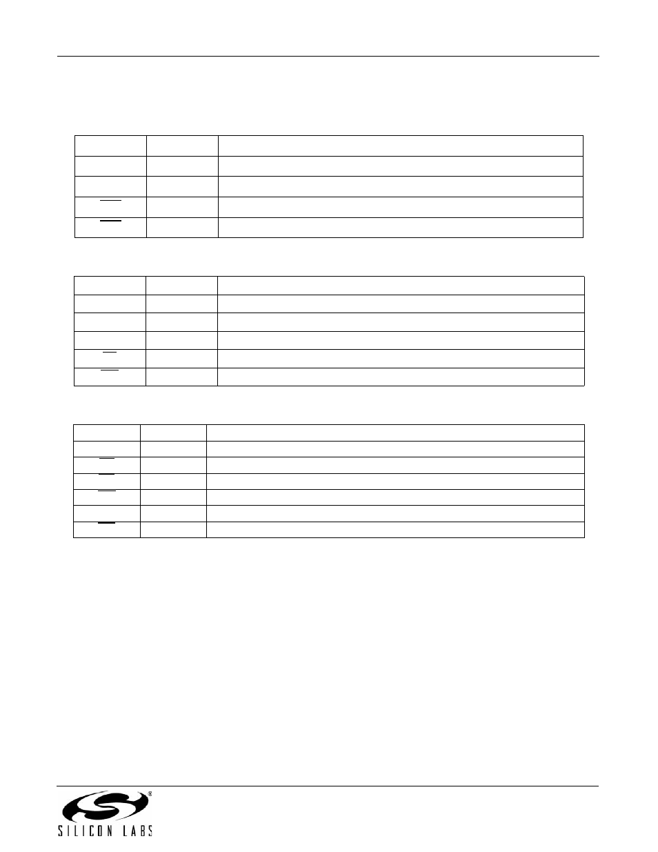
Table 15. UART-Interface Signals
Signal
Direction
Description
TXD
Input
Data input from host TXD pin
RXD
Output
Data output to host RXD pin
RTS
Input
Active-low request-to-send input for flow control
CTS
Output
Clear to send: Si2493 is ready to receive data on the TXD pin (active low)
Table 16. SPI-Interface Signals
Signal
Direction
Description
SCLK
Input
Serial data clock
MISO
Output
Serial data output
MOSI
Input
Serial data input
SS
Input
Chip select (active low)
INT
Output
Interrupt (active low)
Table 17. Parallel-Interface Signals
Signal
Direction
Description
A0
Input
Register selection (address input)
CS
Input
Chip select (active low)
RD
Input
Read enable (active low)
WR
Input
Write enable (active low)
D[7:0]
Bidirectional Parallel data bus
INT
Output
Interrupt (active low)