2 developer’s board overlay, Developer’s board overlay – Sony Ericsson GM47 User Manual
Page 31
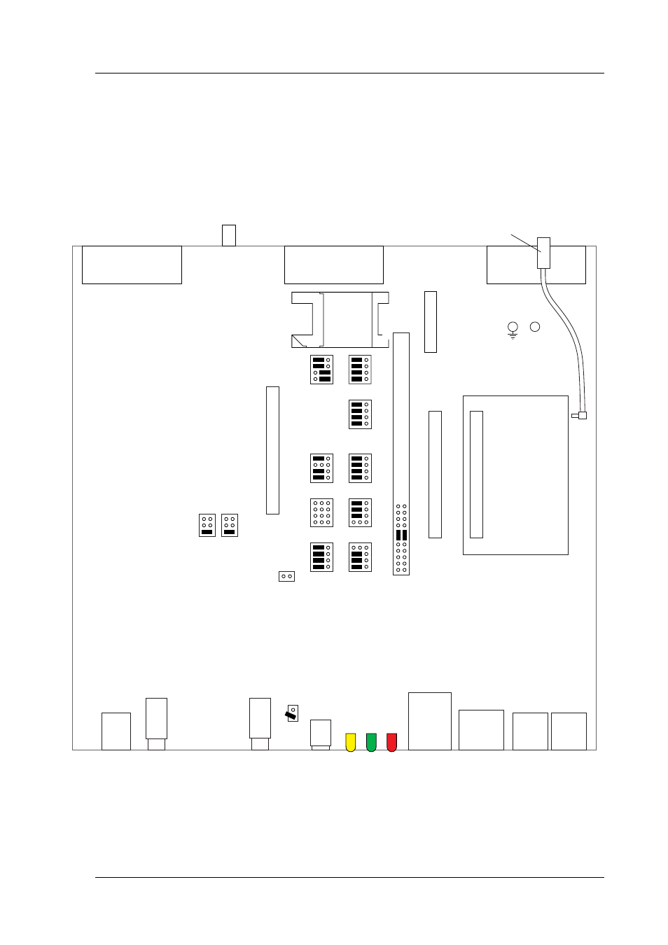
2. USING THE DEVELOPER’S KIT
31
LZT 123 7263 R1C
2.2 Developer’s Board Overlay
Figure 2.3 shows the developer’s board, including the position of all the
connectors, switches and jumpers (default positions). You will notice
that many jumpers are labelled “SW”. This is because the board was
previously fitted with DIL switches.
Figure 2.3 Developer’s board overlay
UART2
(ACB)
UART1
(EDB)
UART3
J5
17
U10
SIM
Holder
TP5 TP4
VCC
J4
1
59
60
2
System Connector
J10
2
60
59
1
System Connector (for flat cable)
J11
2
1
59
60
Te
st Connector
SW8
SW11
SW7
SW10
SW1
SW9
SW6
SW3
SW5
J12
2
60
59
1
Application Connector
JP24
JP21
JP18
12v
DC Power
Socket,
Input
10..15V d.c.
Vcc
NC/OFF/ON
power to
module
ON/OFF
(module)
Handset
PCM
MIC
Audio in
(ATMS)
EAR
Audio out
(AFMS)
SER
VICE
ST
A
T
US
VIO
SIM test
connector
SW4
DCIO
Maintain in
OFF position
(Not used with this module.
Only present for backward
compatibility)
RF connector
Ground stud