Backplaneblade, Clock synchronization interface, Figure – Motorola ATCA-717 User Manual
Page 124: Aaaaaa, Clock synchronization building block

Devices’ Features and Data Paths
Clock Synchronization Interface
124
PENT/ATCA−717
Clock Synchronization Interface
AdvancedTCA systems provide a telecom clock synchronization interface which allows to
synchronize elements within a telecommunication network. The telecom clock
synchronization interface consists of three redundant clock buses (CLK1, CLK2 and
CLK3) which are available at the system backplane. Each clock bus is implemented as a
differential pair of MDS/LDS signals which connects to each system slot.
aaa
In compliance with the AdvancedTCA PICMG 3.0 specification, CLK1 and CLK2 are used
as system clocks and CLK3 is used as reference clock.
a
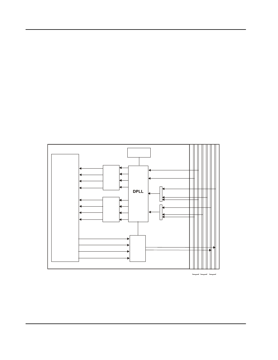
The blade provides a clock synchronization building block which allows to synchronize
the four on−board PMC modules to the system clock and to derive a reference clock. The
main components of the clock synchronization building block as well as the main signal
paths are shown in the following figure.
aaa
A B A B A B
A B
CLK
1
2
3
Backplane
Blade
FPGA
PMC Slots
RCVD_CLK_0
RCVD_CLK_1
RCVD_CLK_2
RCVD_CLK_3
SYNC_0
SYNC_1
SYNC_2
SYNC_3
CLK_0
CLK_1
CLK_2
CLK_3
Clock
Buffer
Clock
Buffer
NET_REF
SYNC_A
SYNC_B
SEC
PRIM
Oscillator
NETREF_B
NETREF_A
SYS_CLK_B
SYS_CLK_A
Figure 38:
Clock Synchronization Building Block
The key component of the clock synchronization building block is the DPLL device
ACS8525 from Semtech. Its main features include:
S Software programmable output clock synthesis (CLK_0, 1, 2, 3)
