Table 6-1. auxiliary supply voltages, Auxiliary supply voltages -3 – KEPCO JQE 150-1.5MVPY-26956 Half Rack User Manual
Page 49
JQE SPECIAL SVC 081111
6-3
2. No D-C Output:
• Check rear terminal block jumper (link) connections for correct placement and tight seat
(Refer to FIG. 5-1).
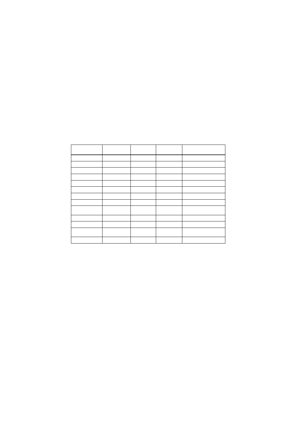
• Check auxiliary supply voltages for A1 and A4 boards for 115V a-c input (see Table 6-1)
1. High D-C Output: If the output voltage is high and not controllable by the voltage control,
identical steps as outlined in step 2 above for No d-c output are advisable. In addition, if the
condition persists, check the following:
• Check the pre-driver transistor* (A1Q1 ) and the main driver (Q305) as well as all pass-
element transistors located on heat sink assembly A3.
• Check the voltage control resistor (R102) for continuity. Monitor output with an oscillo-
scope and observe ripple wave-form and amplitude. If high frequency oscillations are
observed, proceed as directed by PAR. 4.3. High 60 Hz ripple is often due to failure in
one of the rectifier circuits.
2. Input Circuit Breaker Trips at Power-up
• Set the OVP ADJ potentiometer 1/4 turn clockwise.
• For local operation, verify that EOUT LOC-REM switch is set to LOC position (towards
front panel). Verify that link between terminals RVC and RPV1 of TB501 on the rear
panel is installed.
TABLE 6-1. AUXILIARY SUPPLY VOLTAGES
MEASUREMENT
POINT
JQE 15-12MVPY-
26954
JQE 55-5MVPY-
26955
JQE 150-
1.5MVPY-26956
NOTES
A1C2 (–)
–30V ±1.6V
–30V ±1.6V
–30V ±1.6V
Referenced to +S Terminal
A1C10 (+)
+13.5V ±0.7V
+13.5V ±0.7V
+13.5V ±0.7V
Referenced to +S Terminal
A1C11 (–)
–13.5V ±0.7V
–13.5V ±0.7V
–13.5V ±0.7V
Referenced to +S Terminal
A1CR3 cathode
+6.2V ±0.3V
+6.2V ±0.3V
+6.2V ±0.3V
Referenced to +S Terminal
A1CR17 anode
–6.2V ±0.3V
–6.2V ±0.3V
–6.2V ±0.3V
Referenced to +S Terminal
A1C7 (+)
+7.6V ±0.15V
+11.7V ±0.2V
+12.8V ±0.3V
Referenced to +S Terminal
A1CR19 cathode
+6.8V ±0.3V
+6.8V ±0.3V
+6.8V ±0.3V
Referenced to +S Terminal
A1C1 (–)
–16.2V ±0.3V
–16.5V ±0.3V
–16.5V ±0.3V
Referenced to –V Terminal
A1R1 (common
with A1Q1 emitter)
–10.3V ±0.6V
–10.3V ±0.6V
–10.3V ±0.6V
Referenced to –V Terminal
A4C1 (+)
+29.5V ±0.6V
+27.5V ±0.6V
+30.3V ±0.6V
Referenced to –V Terminal
A4CR3 cathode
+15.0V ±0.8V
+15.0V ±0.8V
+15.0V ±0.8V
Referenced to –V Terminal
A4R3 (common
with A4IC1 pin 3)
+6.5V ±0.3V
+6.5V ±0.3V
+6.5V ±0.3V
Referenced to –V Terminal
A4CR10 anode
–6.5V ±0.3V
–6.5V ±0.3V
–6.5V ±0.3V
Referenced to +S Terminal