Table 2–30 – Altera Cyclone IV GX Transceiver Starter Board User Manual
Page 33
Chapter 2: Board Components
2–25
Memory
© March 2010 Altera Corporation
Cyclone IV GX Transceiver Starter Board Reference Manual
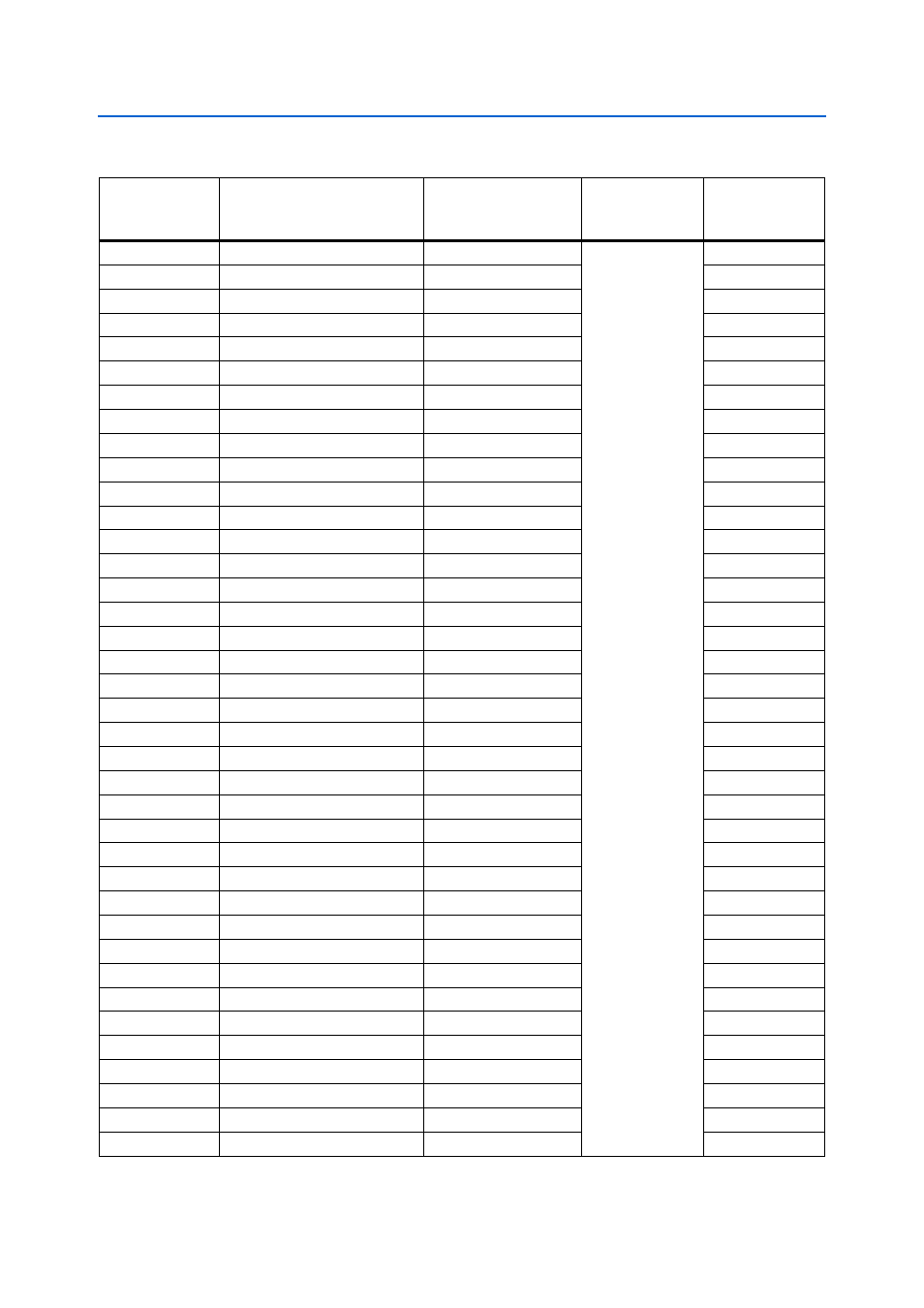
Table 2–30. Flash Pin Assignments, Schematic Signal Names, and Functions (Part 1 of 2)
Board Reference
Description
Schematic Signal Name
I/O Standard
Cyclone IV GX
Device
Pin Number
U11.30
Chip enable
FLASH_CEn
2.5-V
B8
U11.32
Output enable
FSML_OEn
B13
U11.44
Reset
FLASH_RESETn
—
U11.14
Write enable
FSML_WEn
A13
U11.15
Write protect
FLASH_WPn
—
U11.29
Address bus
FSML_A1
A6
U11.25
Address bus
FSML_A2
B6
U11.24
Address bus
FSML_A3
C6
U11.23
Address bus
FSML_A4
A8
U11.22
Address bus
FSML_A5
A7
U11.21
Address bus
FSML_A6
M11
U11.20
Address bus
FSML_A7
N12
U11.19
Address bus
FSML_A8
K10
U11.8
Address bus
FSML_A9
L11
U11.7
Address bus
FSML_A10
M9
U11.6
Address bus
FSML_A11
N10
U11.5
Address bus
FSML_A12
N11
U11.4
Address bus
FSML_A13
H10
U11.3
Address bus
FSML_A14
H12
U11.2
Address bus
FSML_A15
N13
U11.1
Address bus
FSML_A16
M13
U11.55
Address bus
FSML_A17
J13
U11.18
Address bus
FSML_A18
K13
U11.17
Address bus
FSML_A19
L12
U11.16
Address bus
FSML_A20
L13
U11.11
Address bus
FSML_A21
K11
U11.10
Address bus
FSML_A22
K12
U11.9
Address bus
FSML_A23
D13
U11.34
Data bus
FSML_D0
D11
U11.36
Data bus
FSML_D1
D12
U11.39
Data bus
FSML_D2
E10
U11.41
Data bus
FSML_D3
F9
U11.47
Data bus
FSML_D4
E13
U11.49
Data bus
FSML_D5
F10
U11.51
Data bus
FSML_D6
F11
U11.53
Data bus
FSML_D7
G9
U11.35
Data bus
FSML_D8
G10
U11.37
Data bus
FSML_D9
A12