Altera Cyclone IV GX Transceiver Starter Board User Manual
Page 28
2–20
Chapter 2: Board Components
Components and Transceiver Interfaces
Cyclone IV GX Transceiver Starter Board Reference Manual
© March 2010 Altera
Corporation
The PCI Express interface supports a channel width of ×1 as well as the connection
speed of Gen1 at 2.5 Gbps/lane.
The board’s power can be sourced entirely from the PCI Express edge connector when
installed into a PC motherboard. Turn the power switch (SW1) to ON position when
you install the board into a PC motherboard. Although the board can also be powered
by a laptop power supply for use on a lab bench, it is not recommended to use from
both supplies at the same time. Ideal diode power sharing devices have been
designed into this board to prevent damages or back-current from one supply to the
other.
The PCIE_REFCLK_P and PCIE_REFCLK_N signals are a 100-MHz differential input
that is driven from the PC motherboard on this board through the PCI Express edge
connector. This signal connects directly to a Cyclone IV GX REFCLK input pin pair.
This clock is terminated on the motherboard and therefore, no on-board termination is
required. This clock can have spread-spectrum properties that change its period
between 9.847 ps to 10.203 ps. The I/O standard is High-Speed Current Steering Logic
(HCSL).
By default, the GXB_RX0 channel of the FPGA is connected to the PCIE_RX_P and
PCIE_RX_N
signals, while the GXB_TX0 channel is connected to the PCIE_TX_P and
PCIE_TX_N
signals.
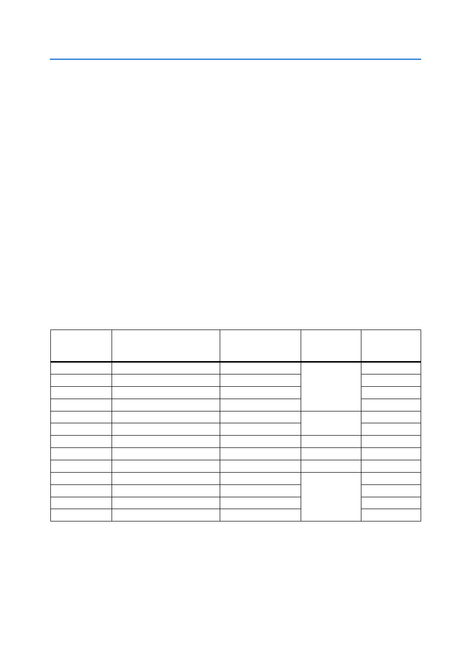
summarizes the PCI Express pin assignments. The signal names and
directions are relative to the Cyclone IV GX FPGA.
Table 2–24. PCI Express Pin Assignments, Schematic Signal Names, and Functions
Board Reference
Description
Schematic Signal Name
I/O Standard
Cyclone IV GX
Device
Pin Number
U14.A16
Add-in card transmit bus
PCIE_TX_P
1.4-V PCML
G2
U14.A17
Add-in card transmit bus
PCIE_TX_N
G1
U14.B14
Add-in card receive bus
PCIE_RX_P
J2
U14.B15
Add-in card receive bus
PCIE_RX_N
J1
U14.A13
Motherboard reference clock
PCIE_REFCLK_P
HCSL
J6
U14.A14
Motherboard reference clock
PCIE_REFCLK_N
J7
U14.A11
Reset
PCIE_PERSTn
LVTTL
A10
U14.A1
Present
PCIE_PRSNTn_x1
—
—
U14.B17
x1 Present
PCIE_PRSNTn_x1
—
—
U14.A5
Motherboard TCK
PCIE_JTAG_TCK
3.3-V
—
U14.A6
Motherboard TDI
PCIE_JTAG_TDI
—
U14.A7
Motherboard TDO
PCIE_JTAG_TDO
—
U14.A8
Motherboard TMS
PCIE_JTAG_TMS
—