I/o resources, I/o resources –5 – Altera Cyclone IV GX Transceiver Starter Board User Manual
Page 13

Chapter 2: Board Components
2–5
Featured Device: Cyclone IV GX Device
© March 2010 Altera Corporation
Cyclone IV GX Transceiver Starter Board Reference Manual
I/O Resources
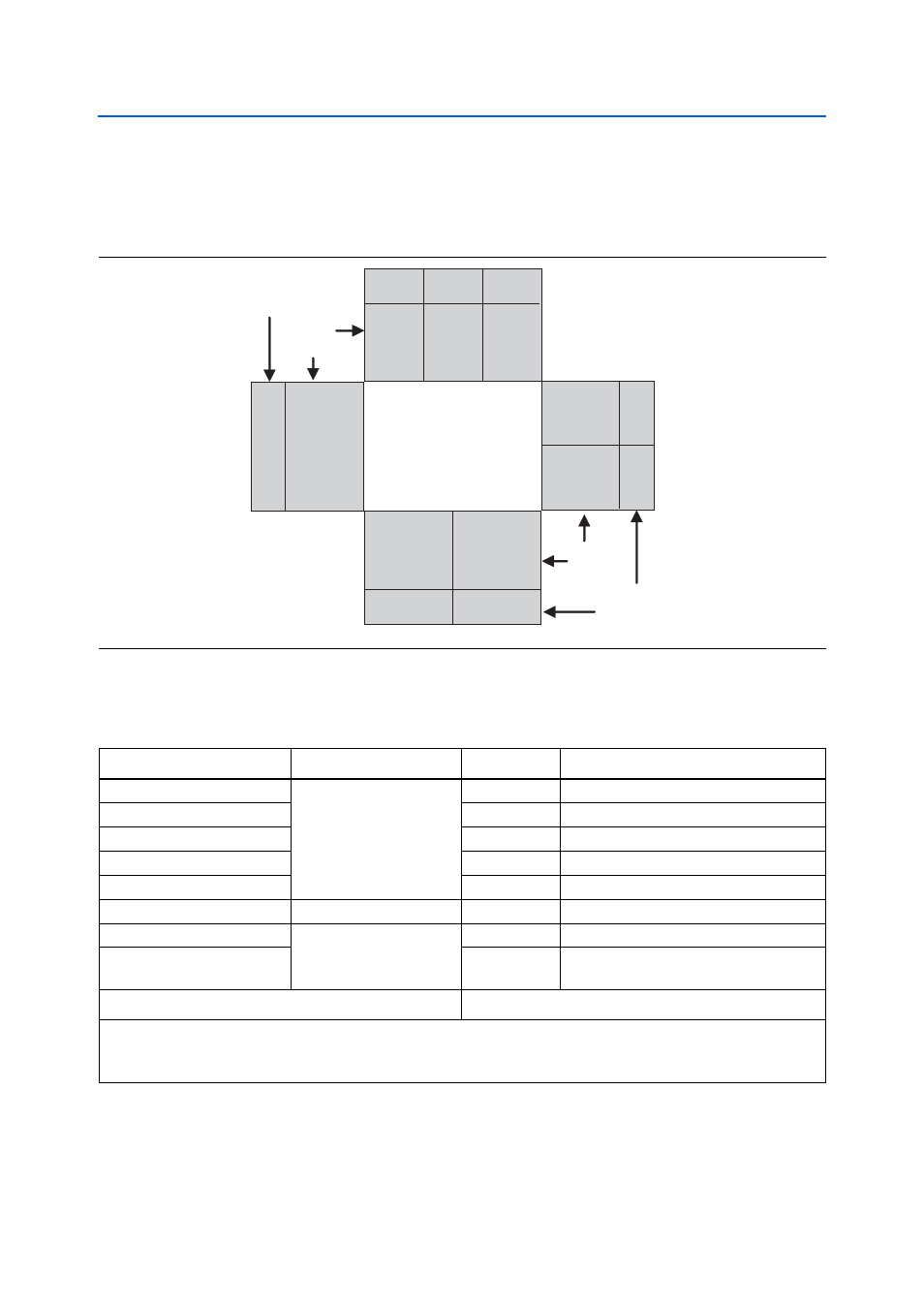
illustrates the bank organization and I/O count for the EP4CGX15BF14
device in the 169-pin FBGA package.
lists the Cyclone IV GX device pin count and usage by function on the
starter board.
Figure 2–2. EP4CGX15BF14 Device I/O Bank Diagram
EP4CGX15
B
a
nk
8
7
1
4
Ba
n
k
4
Bank 6A 12
Ba
n
k
7
1
4
B
a
nk
9
3
1
0
Ba
n
k
3
Bank 5A 12
Bank
Name
Number
of Channels
Bank
Name
Number
of I/Os
2 GXB0
Table 2–4. Cyclone IV GX Device I/O Pin Count and Usage
Function
I/O Standard
I/O Count
Special Pins
Flash, SSRAM, FSML Bus
2.5-V CMOS
47
1 DEV_OE
Gigabit Ethernet
4
—
Buttons
3
1 DEV_CLRn
LCD
1
—
LEDs
4
1 INIT_DONE, 1 nCEO
Clocks or Oscillators
2.5-V CMOS + LVDS
7
3 differential clock input pair, 1 clock input
PCI Express
2.5-V CMOS
1
—
Passive serial and active serial
configuration
4
—
Device I/O Total:
71/72
Notes to
:
(1) 60 out of 72 user I/Os are bidirectional I/O pins while the other 12 pins are for clock inputs only.
(2) The total I/O count excludes the transceiver bank.
