Flash, Flash –24 – Altera Cyclone IV GX Transceiver Starter Board User Manual
Page 32
2–24
Chapter 2: Board Components
Memory
Cyclone IV GX Transceiver Starter Board Reference Manual
© March 2010 Altera
Corporation
lists the SSRAM component reference and manufacturing information.
Flash
The flash interface consists of a single synchronous flash memory device, providing
128-Mb of memory with a 16-bit data bus. This device is part of the shared FSML bus
which connects to the flash memory, SRAM, LCD, and MAX II CPLD EPM2210
System Controller.
f
For more information about the flash memory map storage, refer to th
lists the flash pin assignments, signal names, and functions. The signal
names and types are relative to the Cyclone IV GX device in terms of I/O setting and
direction.
U12.85
Address status controller
SRAM_ADSCn
2.5-V
—
U12.84
Address status processor
SRAM_ADSPn
—
U12.83
Burst address advance
SRAM_ADVn
—
U12.93
Byte lane a write enable
SRAM_BWan
L4
U12.94
Byte lane b write enable
SRAM_BWbn
M4
U12.98
Chip enable
SRAM_CEn
N6
U12.89
Clock
SRAM_CLK
L7
U12.97
Chip enable
SRAM_CE2
—
U12.92
Chip enable
SRAM_CE3n
—
U12.88
Global write enable
SRAM_GWn
—
U12.31
Burst sequence mode selection
SRAM_MODE
—
U12.64
Sleep enable
SRAM_ZZ
—
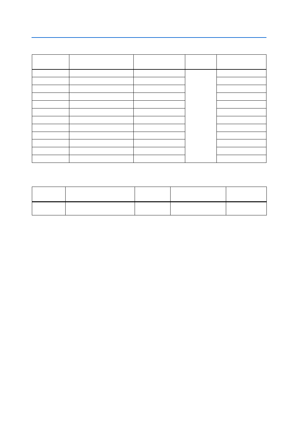
Table 2–28. SSRAM Pin Assignments, Schematic Signal Names, and Functions (Part 2 of 2)
Board Reference
Description
Schematic Signal Name
I/O Standard
Cyclone IV GX Device
Pin Number
Table 2–29. SSRAM Component Reference and Manufacturing Information
Board
Reference
Description
Manufacturer
Manufacturing
Part Number
Manufacturer
Website
U12
Standard Synchronous Pipelined
SCD, 1024 K × 18, 250 MHz
ISSI Inc.
IS61VPS102418A-250TQL