Clock circuitry, Cyclone iv gx transceiver clock inputs, Clock circuitry –16 – Altera Cyclone IV GX Transceiver Starter Board User Manual
Page 24: Cyclone iv gx transceiver clock inputs –16
2–16
Chapter 2: Board Components
Clock Circuitry
Cyclone IV GX Transceiver Starter Board Reference Manual
© March 2010 Altera
Corporation
Clock Circuitry
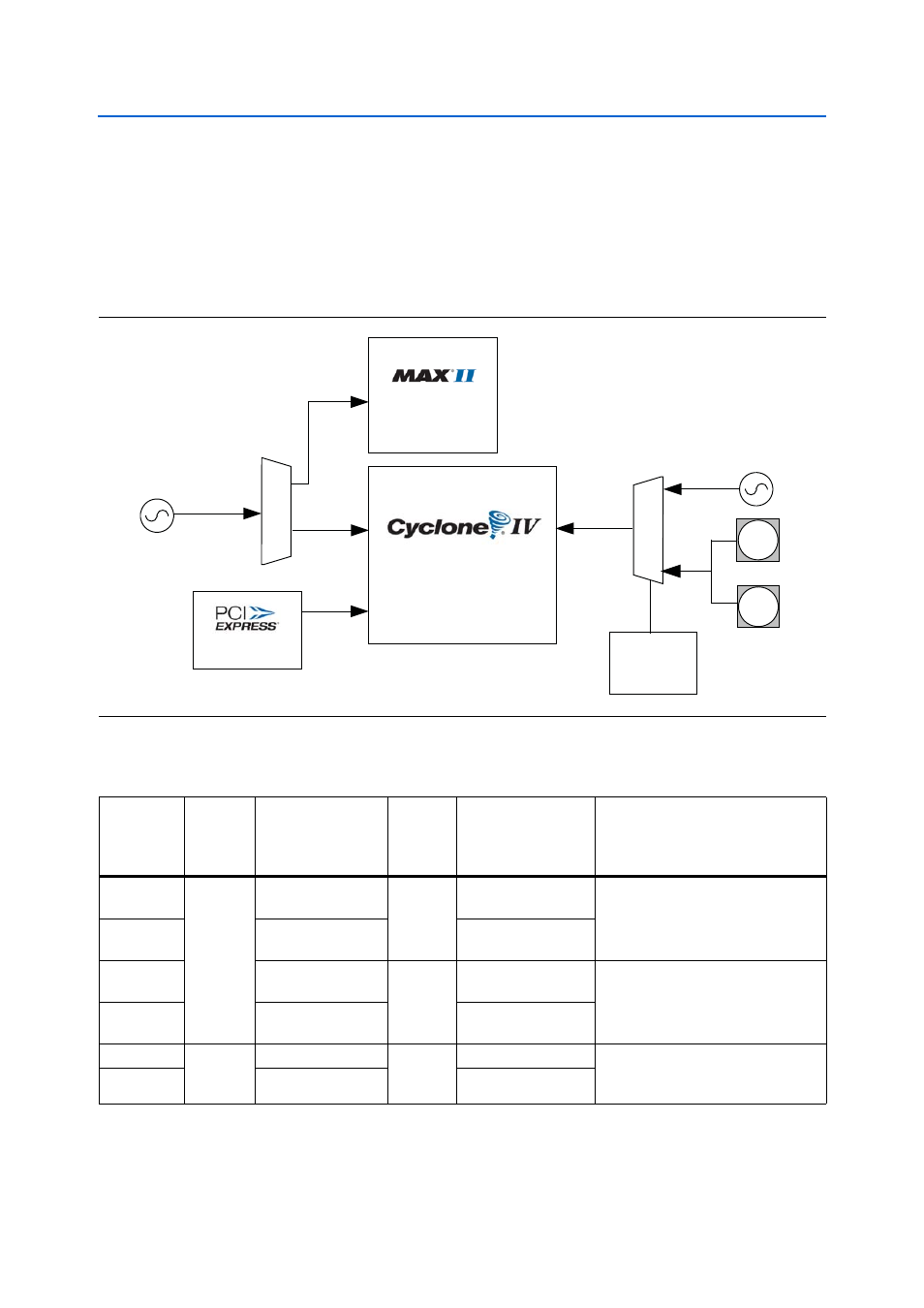
This section describes the board's clock inputs.
Cyclone IV GX Transceiver Clock Inputs
shows the Cyclone IV GX Transceiver starter board clock inputs.
shows the clock inputs for the Cyclone IV GX Transceiver starter board.
Figure 2–5. Cyclone IV GX Transceiver Starter Board Clock Inputs
EP4CGX15F14
SMA
SMA
Clock b
uffe
r
LVDS
Single-Ended
Clock
50 MHz
125 MHz
Source-Select
Switch
Clock b
uffe
r
System Controller
EPM2210F256
LVDS
LVDS
LVDS
CMOS
CMOS
Edge Gold Finger
Table 2–16. Cyclone IV GX Transceiver Starter Board Clock Inputs
Source
Component
Board
Reference
Source
Schematic Signal
Name
I/O
Standard
Cyclone IV GX
Device
Pin Number
Description
J3
SMA or
125 MHz
CLKIN_SMA_P
LVPECL
M7 or E7 depending
on CLK_SEL
Positive and negative differential
LVPECL clock inputs from SMAs.
J2
CLKIN_SMA_N
N7 or E6 depending
on CLK_SEL
X1.4
125M_OCS_P
LVDS
M7 or E7 depending
on CLK_SEL
Positive and negative differential
LVDS clock inputs from 125-MHz
crystal oscillator.
X1.5
125M_OCS_N
N7 or E6 depending
on CLK_SEL
U14.A13
100 MHz
PCIE_REFCLK_P
HCSL
J6
Positive and negative differential
HCSL clock inputs from PCI Express
edge connector.
U14.A14
PCIE_REFCLK_N
J7