Lcd –18, Table 2–19 – Altera Cyclone IV GX Transceiver Starter Board User Manual
Page 26
2–18
Chapter 2: Board Components
General User Input/Output
Cyclone IV GX Transceiver Starter Board Reference Manual
© March 2010 Altera
Corporation
lists the user-defined LED component reference and the manufacturing
information.
LCD
The starter board contains a single 14-pin 0.1" pitch dual-row header that interfaces to
a 16 character × 2 line Lumex LCD display. The LCD has a 14-pin receptacle that
mounts directly to the board's 14-pin header, so it can be easily removed for access to
components under the display. You can also use the header for debugging or other
purposes.
summarizes the LCD pin assignments. The signal names and directions are
relative to the Cyclone IV GX Transceiver.
shows the LCD pin definitions, and is an excerpt from the Lumex data
sheet.
f
For more information such as timing, character maps, interface guidelines, and other
related documentation, visi
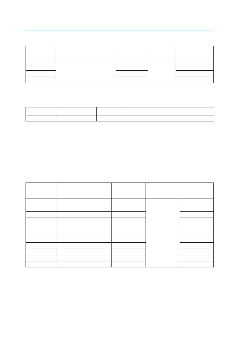
Table 2–19. User-Defined LED Schematic Signal Names and Functions
Board Reference
Description
Schematic
Signal Name
I/O Standard
Cyclone IV GX Device
Pin Number
D8
User-defined LEDs.
Driving a logic 0 on the I/O port turns
the LED ON. Driving a logic 1 on the
I/O port turns the LED OFF.
USER_LED0
2.5-V
N8
D7
USER_LED1
C13
D6
USER_LED2
N5
D5
USER_LED3
M6
Table 2–20. User-Defined LED Component Reference and Manufacturing Information
Board Reference
Device Description
Manufacturer
Manufacturer Part Number
Manufacturer Website
D5 to D8
Green LEDs
Lumex, Inc.
SML-LX1206GC-TR
Table 2–21. LCD Pin Assignments, Schematic Signal Names, and Functions
Board Reference
Description
Schematic Signal
Name
I/O Standard
Cyclone IV GX
Device
Pin Number
J6.5
LCD read or write
FSML_A0
2.5-V
N4
J6.4
LCD register select
FSML_A1
A6
J6.7
LCD data bus
FSML_D0
D11
J6.8
LCD data bus
FSML_D1
D12
J6.9
LCD data bus
FSML_D2
E10
J6.10
LCD data bus
FSML_D3
F9
J6.11
LCD data bus
FSML_D4
E13
J6.12
LCD data bus
FSML_D5
F10
J6.13
LCD data bus
FSML_D6
F11
J6.14
LCD data bus
FSML_D7
G9
J6.6
LCD chip select
LCD_CSn
L9