Altera Parallel Flash Loader IP User Manual
Page 45
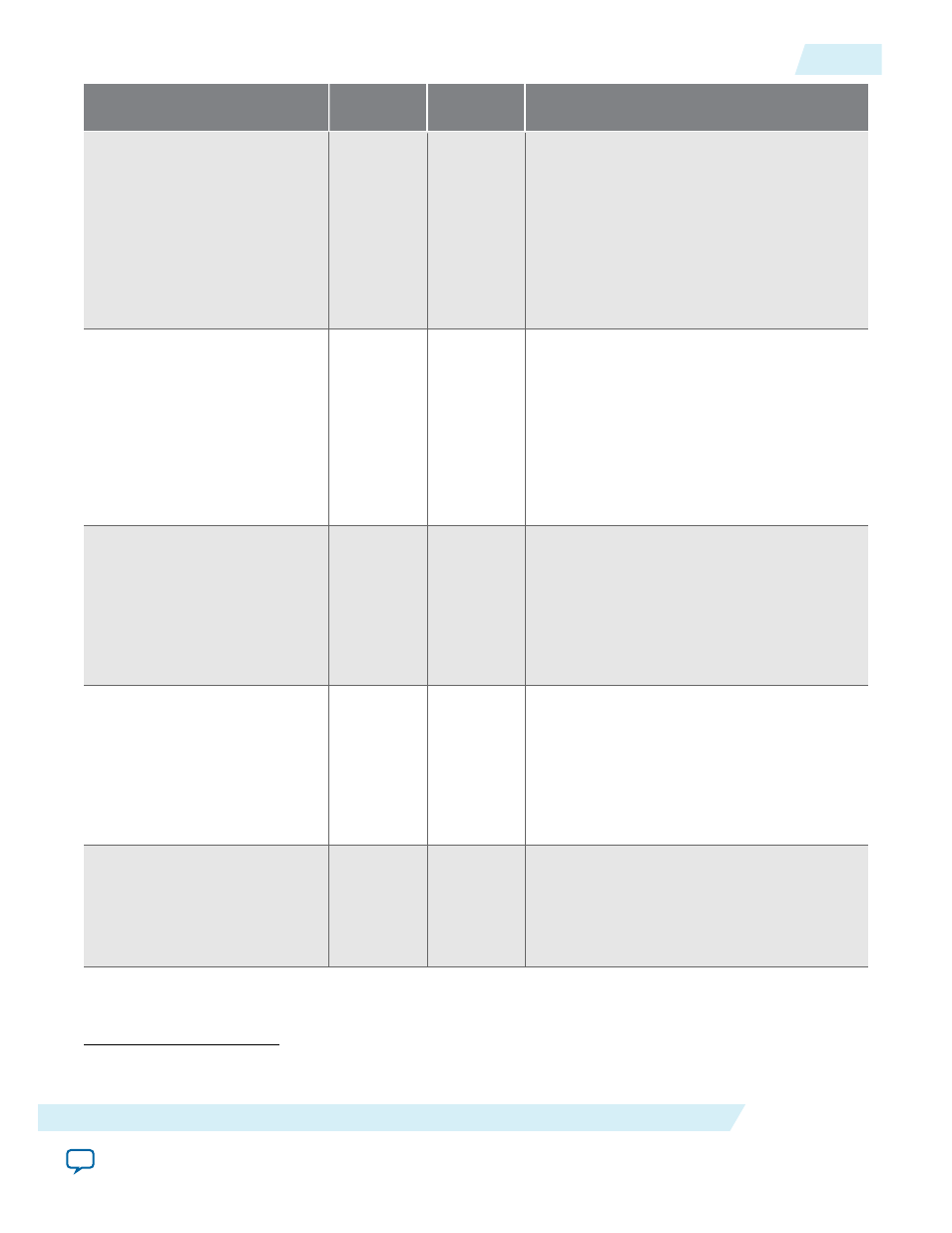
Pin
Description
Weak Pull-
Up
Function
fpga_nstatus
Input
10-kW Pull-
Up Resistor
Connects to the
nSTATUS
pin of the FPGA.
This pin must be released high before the
FPGA configuration and must stay high
throughout FPGA configuration. If a
configuration error occurs, the FPGA pulls
this pin low and the PFL IP core stops
reading the data from the flash memory
device. This pins are not available for the
flash programming option in the PFL IP
core.
pfl_nreconfigure
Input
—
A low signal at this pin initiates FPGA
reconfiguration. You can reconnect this pin
to a switch for more flexibility to set this
input pin high or low to control FPGA
reconfiguration. When FPGA reconfigura‐
tion is initiated, the
fpga_nconfig
pin is
pulled low to reset the FPGA device. The
pfl_clk
. pin registers this signal. This pins
are not available for the flash programming
option in the PFL IP core.
pfl_flash_access_request
Output
—
Used for system-level synchronization.
When necessary, this pin connects to a
processor or an arbitrator. The PFL IP core
drives this pin high when the JTAG interface
accesses the flash or the PFL IP core
configures the FPGA. This output pin works
in conjunction with the
flash_noe
and
flash_nwe
pins.
flash_addr[]
Output
—
Address inputs for memory addresses. The
width of the address bus line depends on the
density of the flash memory device and the
width of the
flash_data
bus. The output of
this pin depends on the setting of the unused
pins if you did not select the PFL interface
tri-state option when the PFL is not
accessing the flash memory device.
flash_data[]
Input or
Output
(bidirection
al pin)
—
Data bus to transmit or receive 8- or 16-bit
data to or from the flash memory in parallel.
The output of this pin depends on the setting
of the unused pins if you did not select the
PFL interface tri-state option when the PFL
is not accessing the flash memory device.
(8)
(8)
Altera recommends not inserting logic between the PFL pins and the CPLD I/O pins, especially on the
flash_data and fpga_nconfig pins.
UG-01082
2015.01.23
Signals
45
Parallel Flash Loader IP Core User Guide
Altera Corporation