Programming quad spi flash – Altera Parallel Flash Loader IP User Manual
Page 10
The PFL IP core provides JTAG interface logic to convert the JTAG stream provided by the Quartus II
software and to program the CFI flash memory devices connected to the CPLD I/O pins.
Figure 4: Programming the CFI Flash Memory With the JTAG Interface
Figure shows an Altera CPLD configured as a bridge to program the CFI flash memory device through the
JTAG interface.
Altera CPLD
CFI Flash
Memory
Altera
FPGA
Configuration Data
Common
Flash
Interface
PFL
Quartus II
Software
via JTAG
Altera FPGA Not Used
for Flash Programming
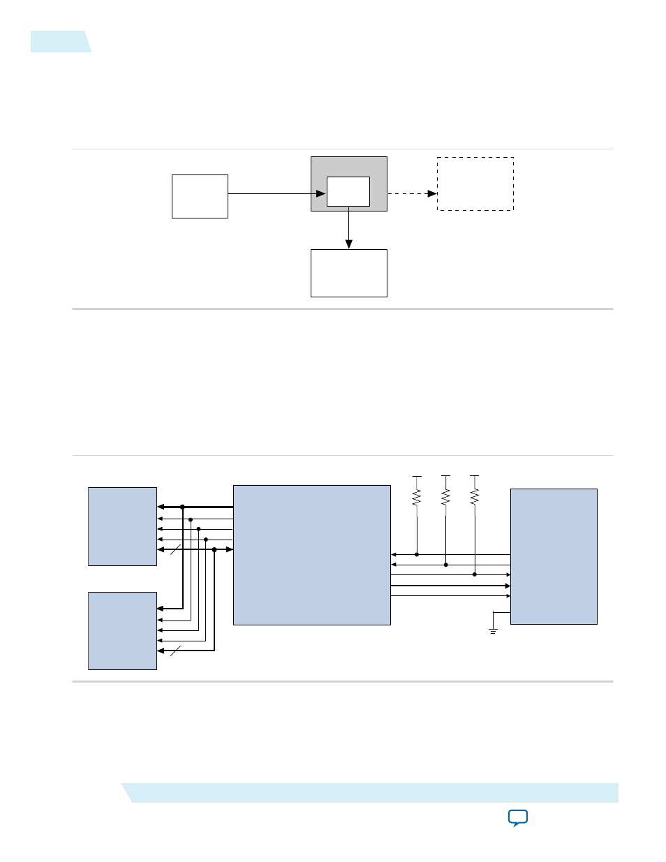
The PFL IP core supports dual P30 or P33 CFI flash memory devices in burst read mode to achieve faster
configuration time. Two identical P30 or P33 CFI flash memory devices connect to the CPLD in parallel
using the same data bus, clock, and control signals. During FPGA configuration, the FPGA DCLK
frequency is four times faster than the flash_clk frequency.
Figure 5: PFL IP core With Dual P30 or P33 CFI Flash Memory Devices
The flash memory devices in the dual P30 or P33 CFI flash solution must have the same memory density
from the same device family and manufacturer. In the Quartus II software version 9.1 SP1 onwards, dual
P30 or P33 flash support is available in the PFL IP core.
VCC
VCC
VCC
P30/P33 CFI Flash
Altera CPLD
Altera FPGA
P30/P33 CFI Flash
16
16
10kΩ
10kΩ
10kΩ
ADDR[24..0]
NCE
NWE
NOE
DATA[15..0]
ADDR[24..0]
NCE
NWE
NOE
DATA[15..0]
flash_addr[24..0]
flash_nce
flash_nwe
flash_noe
flash_data[31..0]
fpga_conf_done
fpga_nstatus
fpga_nconfig
fpga_data
fpga_dclk
CONF_DONE
nSTATUS
nCONFIG
DATA
nCE
DCLK
Programming Quad SPI Flash
You can also use the JTAG interface in Altera CPLDs to program a quad SPI flash memory device with
the PFL IP core.
10
Programming Quad SPI Flash
UG-01082
2015.01.23
Altera Corporation
Parallel Flash Loader IP Core User Guide