Altera Parallel Flash Loader IP User Manual
Page 11
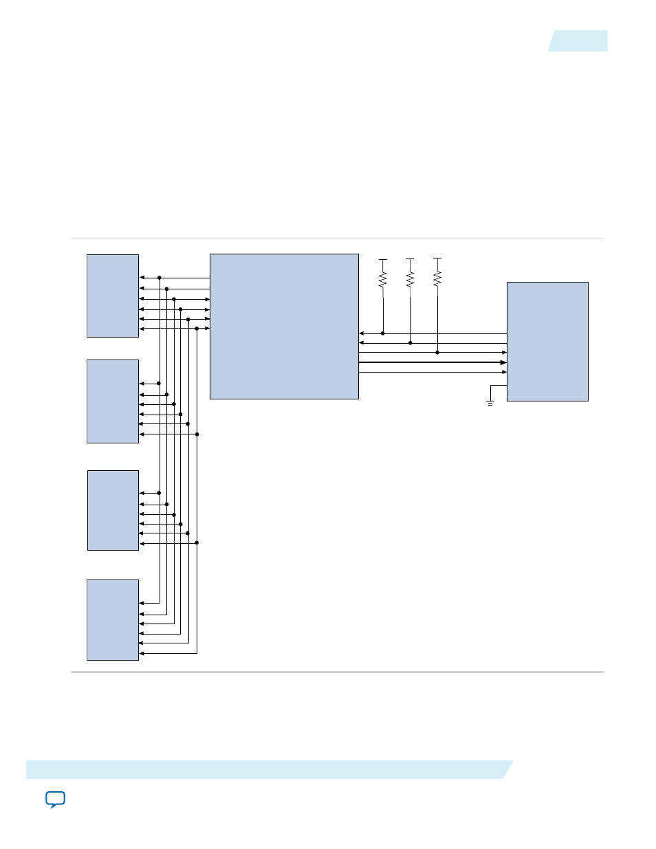
The PFL IP core instantiated in the Altera CPLD functions as a bridge between the CPLD JTAG program‐
ming interface and the quad SPI flash memory device interface that connects to the Altera CPLD I/O pins.
You can connect up to four identical quad SPI flashes in parallel to implement more configuration data
storage.
Note: When connecting quad SPI flashes in parallel, use identical flash memory devices with the same
memory density from the same device family and manufacturer. In the Quartus II software version
10.0 onwards, quad SPI flash support is available in the PFL IP core.
Figure 6: Programming Quad SPI Flash Memory Devices With the CPLD JTAG Interface
Figure shows an Altera CPLD functioning as a bridge to program the quad SPI flash memory device
through the JTAG interface. The PFL IP core supports multiple quad SPI flash programming of up to four
devices.
VCC
VCC
VCC
Quad SPI Flash
Altera CPLD
Altera FPGA
10kΩ
10kΩ
10kΩ
flash_sck
flash_io0
flash_io1
flash_io2
flash_io3
flash_sck[3..0]
flash_io0[3..0]
flash_io1[3..0]
flash_io2[3..0]
flash_io3[3..0]
fpga_conf_done
fpga_nstatus
fpga_nconfig
fpga_data
fpga_dclk
CONF_DONE
nSTATUS
nCONFIG
DATA
nCE
DCLK
flash_ncs
flash_ncs[3..0]
Quad SPI Flash
flash_sck
flash_io0
flash_io1
flash_io2
flash_io3
flash_ncs
Quad SPI Flash
flash_sck
flash_io0
flash_io1
flash_io2
flash_io3
flash_ncs
Quad SPI Flash
flash_sck
flash_io0
flash_io1
flash_io2
flash_io3
flash_ncs
Related Information
Supported Flash Memory Devices
on page 2
UG-01082
2015.01.23
Programming Quad SPI Flash
11
Parallel Flash Loader IP Core User Guide
Altera Corporation