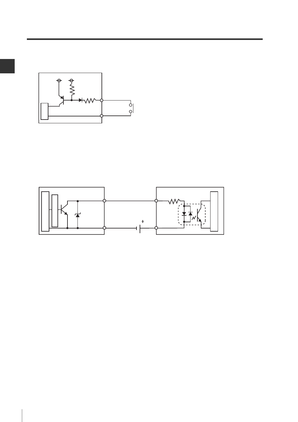
Input circuit diagram – KEYENCE DL-RB1A User Manual
Page 20

18
M
ou
ntin
g an
d Co
nn
ec
tin
g the
D
L-
R
B
1A
2
2-1
Connecting the DL-RB1A to External Devices
Input circuit diagram
Input circuit (Pin Nos. 1 to 5)
* The terminals for pin Nos. 33 and 34 are used in common with 0 V (the blue wire of the sensor
amplifier main unit).
Output circuit (Pin Nos. 6 to 32)
* The terminals for pin Nos. 33 and 34 are used in common with 0 V (the blue wire of the sensor
amplifier main unit).
Main cir
cuit
(Short-circuit current 1 mA max.)
+5V
1 to 5
33 or 34*
Internal circuit
6 to 32 (20 mA max.)
33 or 34*
IN
COM
Photocoupler insulation
PLC etc.
Internal circuit
Overcurrent protect circuit
See also other documents in the category KEYENCE Sensors:
- LR-TB2000 Series (12 pages)
- LR-TB5000 Series (12 pages)
- LR-ZB250AN/AP (4 pages)
- LR-ZB250AN/P (3 pages)
- LR-ZBxN/P Series (3 pages)
- LR-ZBxxB (3 pages)
- OP-85135 (1 page)
- PZ-G Series (2 pages)
- PZ-V/M (2 pages)
- PS-N10 Series (12 pages)
- PX-10 (10 pages)
- CZ-V21A(P) (10 pages)
- CZ-K1(P) (8 pages)
- CZ-V1 (8 pages)
- FS-N10 Series (6 pages)
- FS-N10 Series (116 pages)
- FS-N15CN (1 page)
- FU-93(Z) (2 pages)
- FU-V Series (2 pages)
- FS-V30 (6 pages)
- FU-A40 (1 page)
- NU/FS-N Series (16 pages)
- FS-V33(P) (8 pages)
- FS-V21 (4 pages)
- FS-V22 (4 pages)
- FS-V11(P) (4 pages)
- FS-V1(P) (4 pages)
- LV-N10 Series (12 pages)
- LV-N10 Series (112 pages)
- LV-S62 (1 page)
- OP-84350 (1 page)
- LV-SA (10 pages)
- LV-SB (12 pages)
- OP-87305 (1 page)
- LV Series (10 pages)
- LV-B102 (1 page)
- EV-108M(U) (1 page)
- EZ Series (1 page)
- EM Series (1 page)
- ES-M1(P) (3 pages)
- EX-V Series (120 pages)
- EX-500(W) Series (16 pages)
- GV Series (10 pages)
- IA Series (8 pages)
- LB-1000(W) (24 pages)
