Vmod-2/vmod-2d, Functional description, 5 vmod/vmod-2 connector locations and pin-outs – Kontron VMOD-2D User Manual
Page 38
VMOD-2/VMOD-2D
12/15/97
Functional Description
Page 2 - 12
Man. ID 03139, Rev. Index 0200
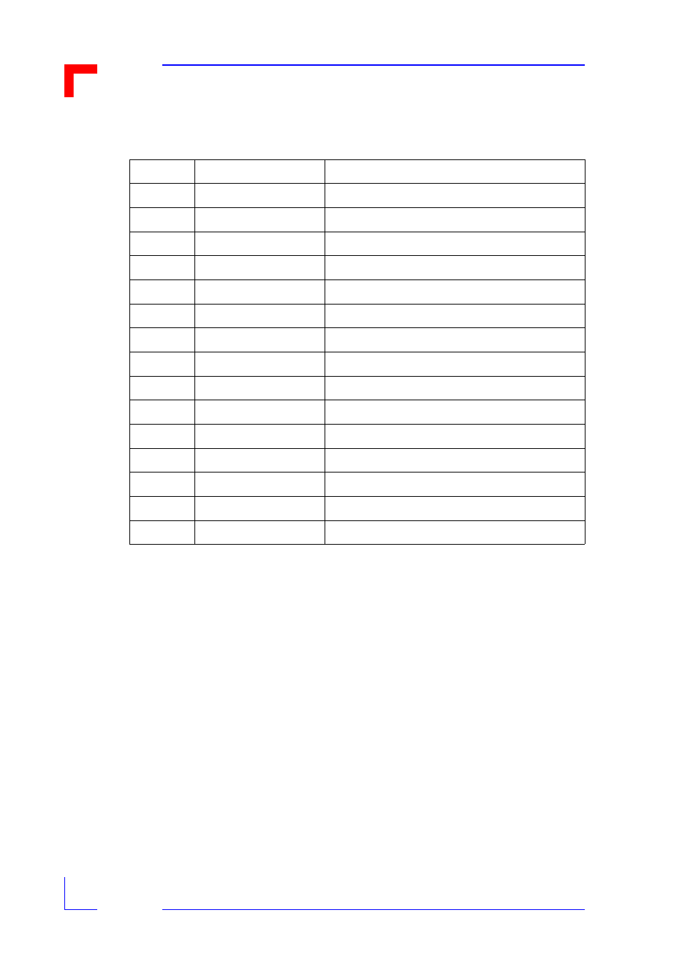
Some ID Bytes you may come across when interrogating your VMOD-2 for it's configuration
are:
As piggybacks are being continually added to the VMOD-2 range, we recommend you check
each employed VMOD/VMOD-2 piggyback's user manual for precise information regarding its
individual ID Byte assignment.
BITBUS is a registered Trademark of the Intel corporation
2.5 VMOD/VMOD-2 Connector Locations and Pin-outs
This section serves to give an overview of the piggyback interface connectors at both the
VMOD-2's VMEbus end and the VMOD-2's (piggyback's) external I/O. Figure 2.4 shows an
example configuration where two piggybacks are to be fitted to your VMOD-2, the first fits in
the upper position (Position A), and the second, is fitted in the lower (B) position. This section
commences with the two header type connectors (BU1a/BU1b and BU0a/BU0b) of the
VMOD-2 which directly interface to the selected piggyback's ST1 and (where 3-row/45-pin
interfaces are used) ST0 pin rows.
The lower case letters in the socket numbers refer to which piggyback location the connector
is used for, i.e. BU1a is socket 1 for piggyback location A. An illustration giving details of all
the VMOD-2's connectors is given below.
Table 2-6: ID Bytes
$EE
PB-BIT
BITBUS™ Communications piggyback
$EF
PB-DIO4
Digital I/O piggyback
$F0
PB-CNT
Counter piggyback
$F1
PB-DAC
D to A converter piggyback
$F1
PB-DAC-2
D to A converter piggyback
$F2
PB-DIO
Digital I/O piggyback
$F3
PB-DIN
Digital Input piggyback
$F4
PB-ADC
A to D converter piggyback
$F5
PB-CIO
Counter/I/O piggyback
$F7
PB-SIO4
Quad serial piggyback
$F8
PB-DOUT
Digital Output piggyback
$F9
PB-DIN2
Digital Input piggyback
$FB
PB-DIO-2
Digital I/O piggyback
$FC
PB-REL
Octo-Relay piggyback
$FD
PB-DIO-3
Digital I/O piggyback
$FE
PB-STP
Digital I/O piggyback