Table 3-4. boost converter characteristics, Table 3-5. led drive characteristics, Table 3-4 – Cirrus Logic CS35L32 User Manual
Page 9: Cs35l32
DS963F4
9
CS35L32
3 Characteristics and Specifications
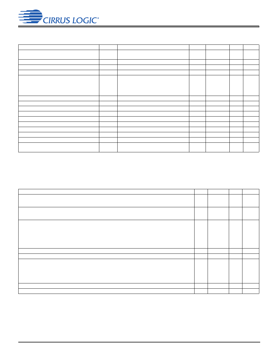
Table 3-4. Boost Converter Characteristics
Test conditions, except where noted otherwise: VA = 1.8 V, VP = 3.6 V, VBST = 5.0 V, amp gain = 12 dB, GNDA = GNDP = 0 V, TA = +25°C
,
MCLK
INT
= 6 MHz. MCLK
INT
is explained in
Parameters Symbol
Test
Conditions
Min
Typical
Max
Units
Boost output voltage
VBST
Boosting
Bypass
VP*1.15
—
—
VP
5.4
—
V
V
Boost output voltage tolerance
VBST
No load: I
LOAD
=0 mA
–5
—
+5
%
Load regulation
V
(Load)
3.0 V < VP < 4.2 V; I
LOAD
= 0.25A to1.5 A
—
60
—
mV/A
Line regulation
V
(Line)
3.0 V LOAD = 0 A, 500 mA — 40 — mV/V Boost FET peak-current limit .) I MAX(B) BST_IPK = 0000 0000 BST_IPK = 0010 0000 BST_IPK = 0100 0000 BST_IPK = 0110 0000 BST_IPK = 1000 0000 — — — — — 2.89 3.30 3.72 4.14 4.56 — — — — — A A A A A Output switching frequency 1 1. ) should be configured so MCLK INT is 6 or 6.1440 MHz (see ) for boost-converter operation at 2 or 2.05 MHz. f SW(B) — — MCLK INT /3 — MHz Boost FET ON resistance R DS(ON)B I OUT(B) = 1 A — 80 — m Boost FET ON resistance temp coefficient — I OUT(B) = 1 A — 0.2 — %/ o C Rectifying FET ON resistance R DS(ON)R I OUT(B) = 1 A — 150 — m Rectifying FET ON resistance temp coefficient I OUT(B) = 1 A — 0.2 — %/ o C Overvoltage detection threshold V OVTH Boost enabled — 5.5 5.7 V Threshold Class G On, IN+ to IN– V IN1THON VBST = VP = 3.6 V — 0.60 — V Threshold Class G Off, IN+ to IN– V IN1THOF VP = 3.6 V, VBST = 5 V — 0.33 — V Minimum Class G boost ON hold-off time — VP = 3.6 V, VBST = 5 V — 800 2 2.Minimum Class G boost ON hold-off time is determined from when the low audio detection is latched until when the boost is turned off. The latching mechanism occurs in 800-ms intervals. If the audio level is detected as low between two sequential latches, the hold-off time is extended by the — ms Operating efficiency 3 3.Efficiency specified here assumes the boost converter drives an external resistive load via the VBST pin, instead of the onboard Class D amplifier. B VBST = 5 V, I OUT(B) = 500 mA VBST = 5 V, I OUT(B) = 1.5 A — 90 — % Table 3-5. LED Drive Characteristics Test conditions, except where noted otherwise: VA = 1.8 V, VP = 3.6 V, VBST = 5.0 V, GNDA = GNDP = GNDPLED = 0 V, TA = +25°C . Parameters Min Typical Max Units Flash Mode current settings, per LED 1 (Step size = 50 mA) 1.Flash or Movie Mode current is delivered from the boost converter’s output, which provides a voltage higher than the LED voltage. Depending on the LED voltage requirement and on VP supply voltage, the boost converter is internally controlled to boost or be in bypass (rectifying FET fully on). LED_FLCUR = 1111 … LED_FLCUR = 0001 — … — 750 … 50 — … — mA … mA Flash Inhibit Mode current settings, per LED (Step size = 50 mA) LED_FLINHCUR = 0111 … LED_FLINHCUR = 0001 — … — 350 … 50 — … — mA … mA Movie Mode current settings, per LED LED_MVCUR = 111 LED_MVCUR = 110 LED_MVCUR = 101 LED_MVCUR = 100 LED_MVCUR = 011 LED_MVCUR = 010 LED_MVCUR = 001 — — — — — — — 150 120 100 80 60 40 20 — — — — — — — mA mA mA mA mA mA mA LED current accuracy –10 — +10 % LED current matching — 10 — % Flash timer (t flash ) MCLK INT = 6 MHz 2 ; TIMER = 1 0010–1 1111 TIMER = 0 0001 TIMER = 0 0000 MCLK INT = 6.144 MHz; TIMER = 1 0010–1 1111 TIMER = 0 0001 TIMER = 0 0000 2.The flash time setting is generated from MCLK INT ) should be configured so MCLK INT is 6 or 6.1440 MHz. See . — — — — — — 500 75 50 488.3 73.2 48.8 — — — — — — ms ms ms ms ms ms LED flash timer accuracy 0 — +1 ms LED flash inhibit time (FLINH high to LED current 3% settling) — 40 — s
(See
difference between when the detection occurs and the subsequent latch pulse. This may extend the hold-off time up to 1.6 s in extreme cases.
—
85
—
%