6 power control 2, 7 clocking control, 8 low battery thresholds – Cirrus Logic CS35L32 User Manual
Page 37: Section 7.7, Mclkdiv2, P. 37, Section 7.6, Any d, Lowbat_th, Lowbat_recov
DS963F4
37
CS35L32
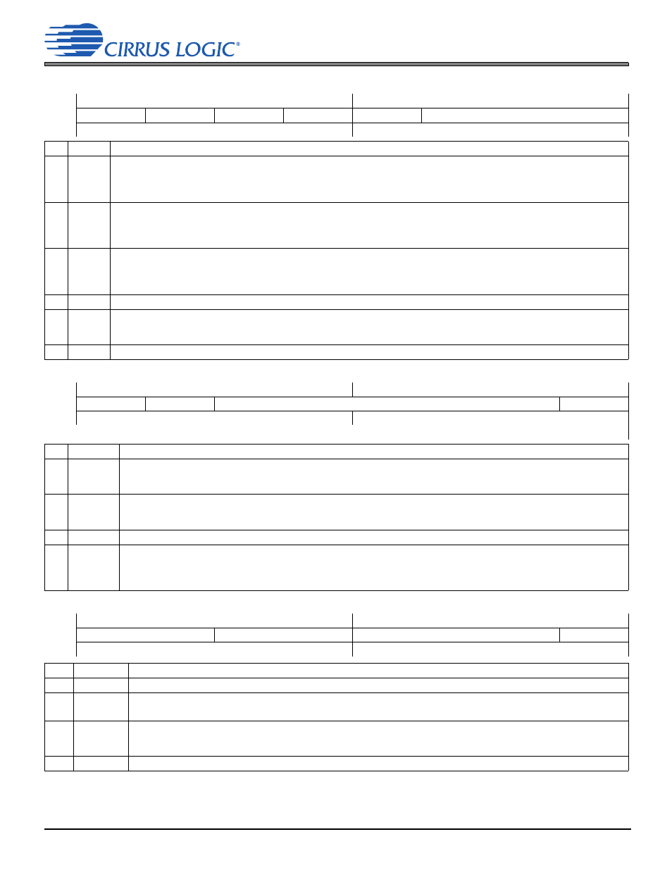
7.6 Power Control 2
7.6 Power Control 2
Address 0x07
R/W
7
6
5
4
3
2
1
0
PDN_VMON
PDN_IMON
PDN_VPMON
—
SDOUT_3ST
—
Default
1
1
1
0
1
0
0
0
Bits
Name
Description
7
PDN_
VMON
Power-down VMON ADC. Configures the power state of the ADC front end and the ADC used to monitor the VSENSE± input
pins to create the VMON data.
0 Powered up
1 (Default) Powered down
6
PDN_
IMON
Power-down IMON ADC. Configures the power state of the ADC front end, and the ADC, and range selection circuitry used to
monitor the ISENSE± input pins to create the IMON data.
0 Powered up
1 (Default) Powered down
5
PDN_
VPMON
Power-down VPMON ADC. Configures the ADC front end power state and the ADC used to monitor the VP supply pin to create
the VP data.
0 Powered up
1 (Default) Powered down
4
—
Reserved
3
SDOUT_
3ST
Tristate the ADSP SDOUT path. Configures the Hi-Z state of the ADSP SDOUT output path.
0 SDOUT is powered up.
1 (Default) SDOUT is Hi-Z.
2:0
—
Reserved
7.7 Clocking Control
Address 0x08
R/W
7
6
5
4
3
2
1
0
MCLKDIS
MCLKDIV2
—
RATIO
Default
0
1
0
0
0
0
0
0
Because clock rates must be stable when the device is powered up, the device must be powered down before changing clock rates.
Bits
Name
Description
7
MCLKDIS MCLK disable. Configures the state of MCLK
INT
before its fan-out to all the internal circuitry.
0 (Default) On
1 Off. Disables the clock tree to save power when the device is powered down. Set only after the device powers down.
6
MCLKDIV2 MCLK divide by 2. Configures a divide between the input pin MCLK and the derived core clock, MCLK
INT
.
0 No divide
1 (Default) Divide by 2
5:1
—
Reserved
0
RATIO
f
MCLK(INT)/
f
LRCK
ratio.
shows the effect of these settings on the Master Mode duty cycle.
0 (Default)128
1 125
Application: Refer to
Section 4.11.2, “Master and Slave Timing.”
7.8 Low Battery Thresholds
Address 0x09
R/W
7
6
5
4
3
2
1
0
—
LOWBAT_TH[1:0]
LOWBAT_RECOV[2:0]
—
Default
0
0
1
0
0
1
1
0
Bits
Name
Description
7:6
—
Reserved
5:4
LOWBAT_
TH
Low battery nominal threshold, falling VP. See
for accuracy specifications.
00 3.1 V
01 3.2 V
10 (Default) 3.3 V
11 3.4 V
3:1
LOWBAT_
RECOV
Low battery nominal recovery threshold, rising VP. See
for accuracy specifications.
000 Reserved
001 3.2 V
010 3.3 V
011 (Default) 3.4 V
100 3.5 V
101 3.6 V
110–111 3.6 V
0
—
Reserved.