3 audio and led operation, 11 audio/data serial port (adsp), 1 power up, power down, and tristate – Cirrus Logic CS35L32 User Manual
Page 24: Section 4.11, Audio/data, Serial port, Adsp), Section 4.10.3, Described in, Cs35l32
24
DS963F4
CS35L32
4.11 Audio/Data Serial Port (ADSP)
4.10.3 Audio and LED Operation
When audio and LEDs are operating simultaneously, the user can select one the following courses of action:
• By clearing AUDIOGAIN_MNG, if the CS35L32 enters load management mode due to the conditions listed in
, audio gain is reduced once by 3 dB (no reduction for 9-dB gain). If the condition persists, the CS35L32
examines ILED_MNG and responds according to
. Audio automatically recovers to the original
volume after an LED event.
• By setting AUDIOGAIN_MNG, the user maintains full control over audio gain.
As a default, the boost converter’s output voltage is fixed in Bypass Mode (VBST = VP). The user can set VBOOST_MNG
to any of the nondefault modes for a different boost behavior. In particular, if VBOOST_MNG = 01 in the presence of LED
and audio load power, the CS35L32 adapts for low-power dissipation by automatically reducing the LED driver voltage at
pins FLOUT1 and FLOUT2 and by reducing the boost converter’s output voltage. If VBOOST_MNG = 00 in the presence
of LED and audio-load power, the boost converter’s output voltage is determined by the higher of the two supply
requirements for LED or audio Class G. In such a case, the CS35L32 cannot adapt for low power dissipation if audio
Class G requires a 5-V supply, because of the higher audio signal. Refer to
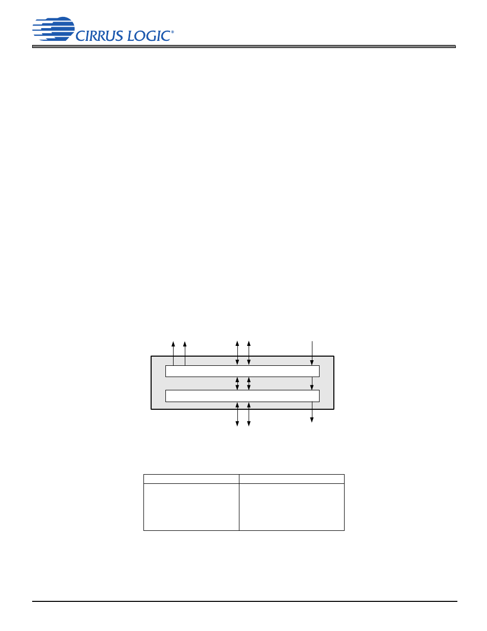
4.11 Audio/Data Serial Port (ADSP)
The ADSP transmits audio and data to and from the systems processor in traditional I²S Mode. Controls are provided to
advise the device of the rate of the clocks being applied to its inputs when in Slave Mode. Likewise, the same controls are
used to indicate the clock rates to be generated when operating as a clock master.
The serial port I/O interface consists of three signals, described in detail in
• SCLK: Serial data shift clock
• LRCK: Provides the left/right clock, which identifies the start of each serialized data word and toggles at sample rate
• SDOUT: Serial data output
Figure 4-9. Audio/Data Serial Port (ADSP)
provides links to register fields used to configure components shown in
.
4.11.1 Power Up, Power Down, and Tristate
The serial port has separate power-down and tristate controls for its output data path (
, see
master/slave operation is governed only by the
), irrespective of the SDOUT_3ST setting.
describes ADSP operational mode and pin-output driver-state configuration.
Table 4-5. ADSP Configuration
Register Field
Cross-Reference to Description
PDN_AMP
SDOUT_3ST
MCLKDIS, MCLKDIV2, RATIO
M/S
M_ADSPCLK_ERR
ADSPCLK_ERR
Section 7.5
Section 7.6
Section 7.7
Section 7.13
Section 7.16
Section 7.19
Level Shifters
Audio Data Serial Port
From Signal
Monitoring Blocks
R
Onchip Channel
Select
LRCK SCLK
Onchip Serial Port
Rate Control
L
LRCK SCLK
SDOUT