1 pin descriptions, Cs35l32 – Cirrus Logic CS35L32 User Manual
Page 5
DS963F4
5
CS35L32
1 Pin Descriptions
1 Pin Descriptions
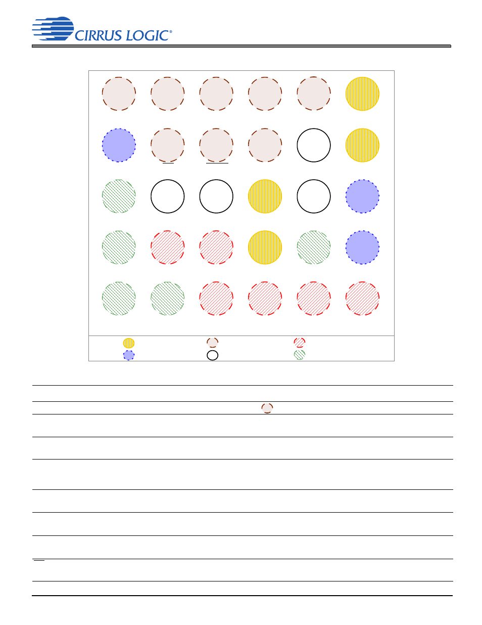
Figure 1-1. Top-Down (Through-Package) View—30-Ball WLCSP Package
‘
‘
‘
‘
‘
‘
‘
‘
‘
‘
‘
‘
‘
‘
‘
‘
‘
‘
‘
‘
‘
‘
‘
‘
‘
Table 1-1. Pin Descriptions
Ball Name
Ball
Number
Power
Supply I/O
Ball Description
Internal
Connection
Driver
Receiver State at
Reset
SDA
VA
I/O I
2
C
Serial Data Input. Serial data for the I
2
C
serial port
—
CMOS
open-drain
output
Hysteresis
on CMOS
input
Hi-Z
SCL
VA
I I
2
C
Clock Input. Serial clock for the I
2
C serial
port
—
—
Hysteresis
on CMOS
input
Hi-Z
MCLK
VA
I Master Clock Source. Clock source for A/D
converters and audio/data serial port (ADSP).
MCLK
INT
, derived from MCLK, is used for other
blocks (see
).
Weak pull-
down
(~1 M
—
Hysteresis
on CMOS
input
Pulled
down
SCLK
VA
I/O Serial Clock. Serial shift clock for the serial
audio interface
Weak pull-
down
(~1 M
CMOS
output
Hysteresis
on CMOS
input
Pulled
down
LRCK
VA
I/O Left Right Clock. Determines which channel,
left or right, is currently active on the serial
audio/data lines
Weak pull-
down
(~1 M
CMOS
output
Hysteresis
on CMOS
input
Pulled
down
SDOUT
VA
O Serial Audio/Data Output. I²S serial data
output used to monitor voltage and current of
SPKOUT signal and VP levels
Weak
pull-down
(~1 M
CMOS
output
—
Pulled
down
INT
VA
O Interrupt. Programmable, open-drain, active-
low programmable interrupt output
—
CMOS
open-drain
output
—
Hi-Z
A1
A2
A3
A4
A5
A6
B1
B2
B3
B4
B5
B6
C1
C2
C3
C4
C5
C6
D1
D2
D3
D4
D5
D6
E1
E2
E3
E4
E5
E6
General Ground
LED
Digital I/O
Power Supply
Boost Converter
Audio
Digital I/O