Cs35l32 – Cirrus Logic CS35L32 User Manual
Page 10
10
DS963F4
CS35L32
3 Characteristics and Specifications
Table 3-6. Speaker Amplifier Output Characteristics
Test conditions, except where noted otherwise: VA = 1.8 V, VP = 3.6 V, VBST = 5.0 V, 1-kHz input, amp gain = 12 dB, GNDA = GNDP = 0 V, T
A
= +25°C,
measurement bandwidth is 20 Hz to 20 kHz, Fs = 48 kHz, MCLK
INT
= 6 MHz. MCLK
INT
is explained in
Parameters
Symbol Test
Conditions
Min
Typical Max Units
Continuous average power delivered to load
1
1.Power delivered to the speaker from the 0.1-
load side terminal (refer to
).
Po
8-
load, THD 10%
8-
load, THD 1%
—
—
1.75
1.45
—
—
W
W
THD+N
THD+N
8-
load, 1.0 W —
0.02
—
%
Input voltage @ 1% THD+N
V
ICLIP
8-
load —
0.84
—
Vrms
Signal to noise ratio
SNR
Referenced to output voltage @1% THD+N, A-weighted —
102
—
dB
Idle channel noise
ICN
VBST = VP, A-weighted —
25
—
Vrms
Common-mode rejection ratio
CMRR
V
ripple
= 1 V
PP
, f
ripple
= 217 Hz —
55
—
dB
Frequency response
FR
20 Hz to 20 kHz, No input DC blocking caps –0.1
0
0.1
dB
Efficiency
2
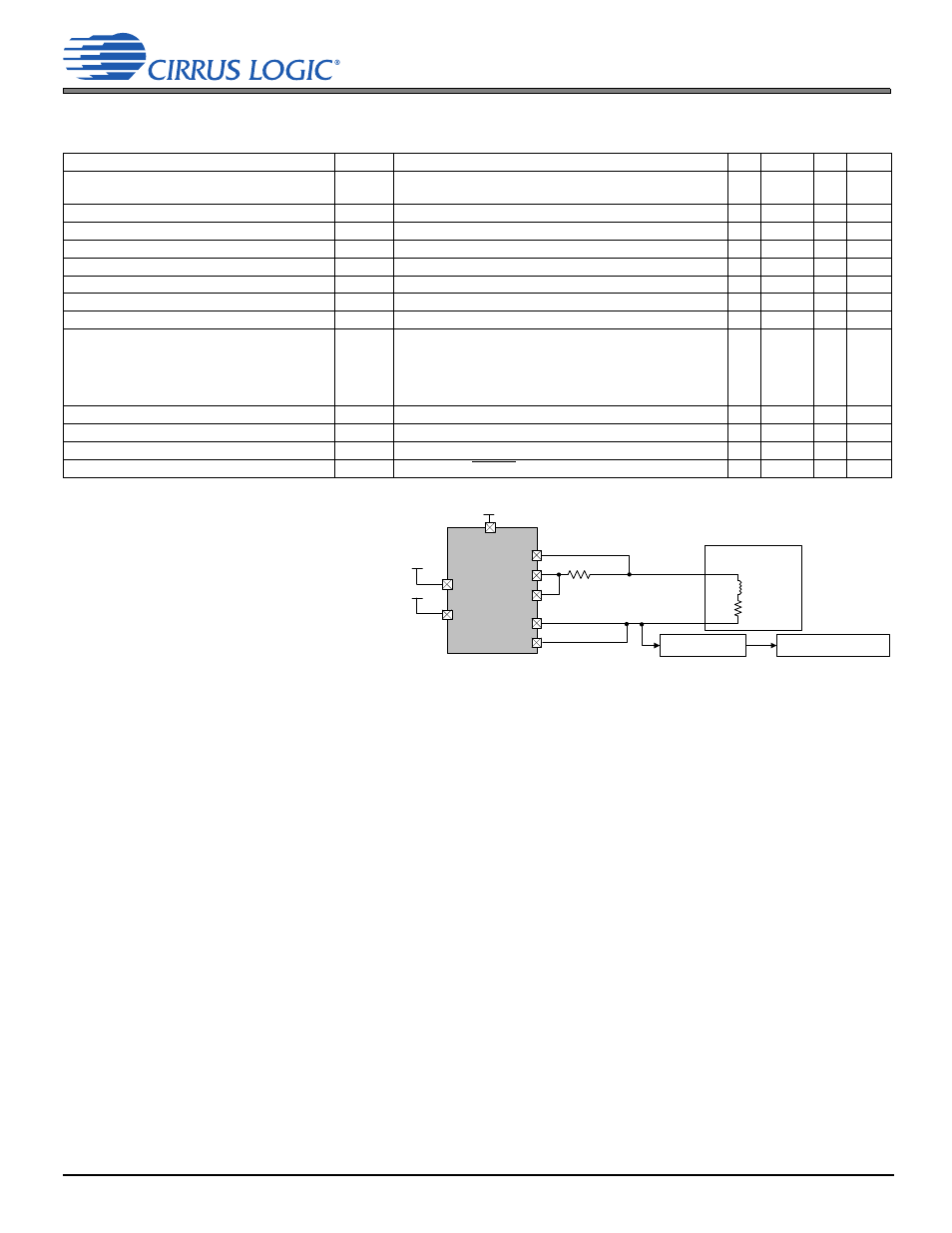
2.Efficiency collected using a 5-V external supply, as shown
in the drawing. For this test, the VBST pin should not be
connected to the SPKRSUPPLY pin.
A
8-
load 33 H, 1.7 W —
91
—
%
Class D amplifier gain
—
AMP_GAIN = 000 (mute)
AMP_GAIN = 001
AMP_GAIN = 010
AMP_GAIN = 011
AMP_GAIN = 100
—
—
—
—
—
–80
9
12
15
18
—
—
—
—
—
dB
dB
dB
dB
dB
N-FET ON resistance
R
DS ON,N
I
FET
= 0.5 A —
185
—
m
P-FET ON resistance
R
DS ON,P
I
FET
= 0.5 A —
205
—
m
Output DC offset voltage
V
OFFSET
Inputs AC coupled to ground —
±5
—
mV
Time from shutdown to audio out
t
SD
RESET deasserted, zero-crossing disabled —
15
—
ms
Generic Simulated
Speaker Load
R
SENSE
0.1
Audio Precision AP 2700
Audio Analyzer
Audio Precision
AUX-0025 Filter
SPKOUT+
ISENSE+
SPKOUT–
ISENSE–/
VSENSE+
VSENSE–
SPKRSUPPLY
5 V
3.6 V
1.8 V
VP
VA
8
33
H