Section 4.12.3, Cs35l32 – Cirrus Logic CS35L32 User Manual
Page 28
28
DS963F4
CS35L32
4.12 Signaling Format
4.12.3 Transmitting Data from a Dual-CS35L32 Configuration
To indicate a dual-CS35L32 configuration where the SDOUT line is shared, the user must set
(see
). When
two CS35L32 devices are available on the same board, each device is identified by its I
2
C address. The AD0 pin is shared
by FLOUT2. Upon power-up or upon deasserting RESET, each CS35L32 reads the AD0 pin logic level and configures its
chip address. Transmission starts when
) is cleared. The Device 0 address (AD0 level low)
transmits its data on the left channel time slot while Device 1 is automatically tristated; the Device 1 address (AD0 level
high) transmits on the right-channel time slot while Device 0 is automatically tristated.
The
) determines data transmission for both CS35L32s, as shown below:
•
(DATCNF = 00): left and right channel VMON[11:0], IMON[11:0], VPMON[7:0]
•
(DATCNF = 01): left and right channel VMON[11:0], IMON[11:0], STATUS
•
(DATCNF = 10): left and right channel VMON[15:0], IMON[15:0]
•
(DATCNF): left and right channel VPMON[7:0], STATUS
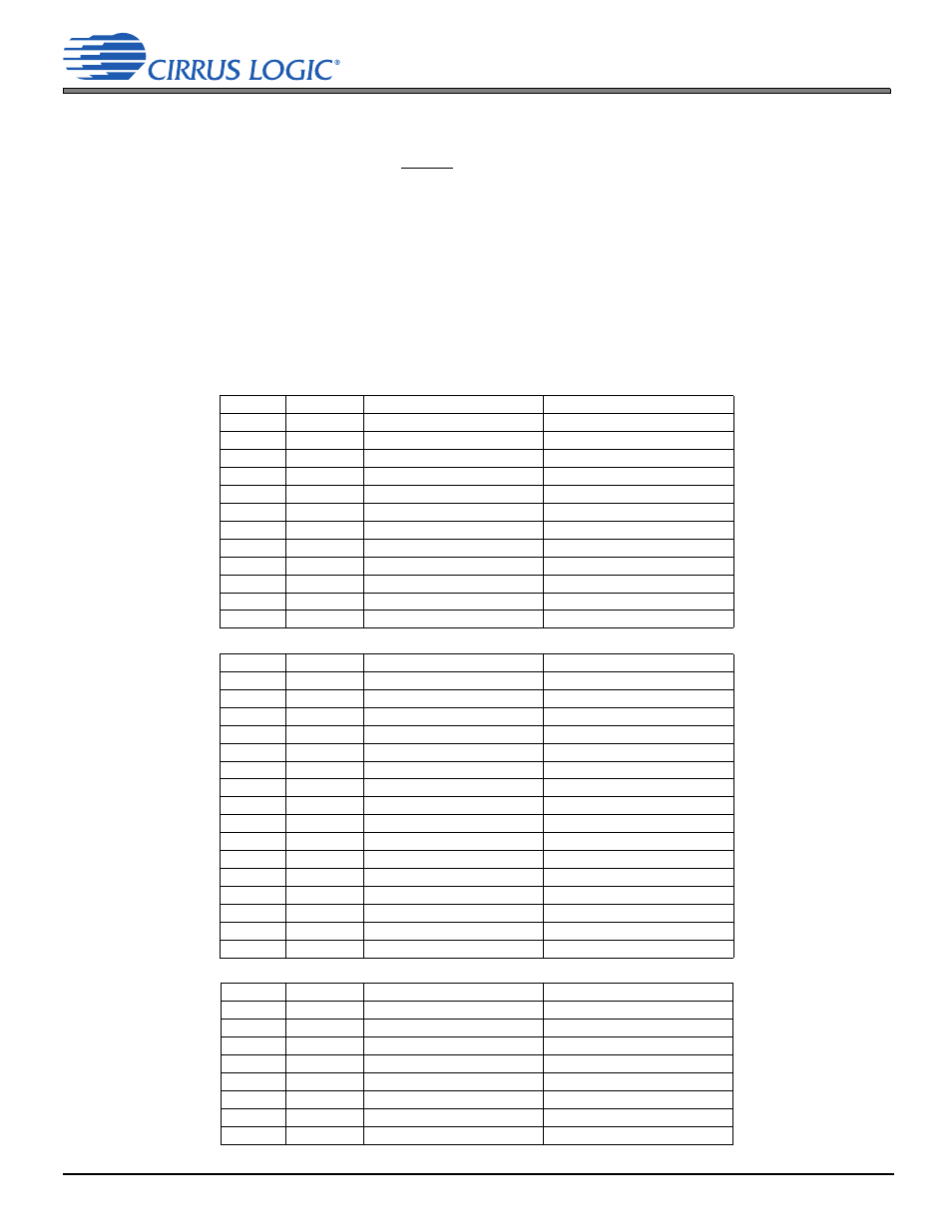
Table 4-10. SDOUT Monitor Data Positioning (Two CS35L32s, DATCNF = 00)
Bit
Bit Number Left-Channel Data Contents Right-Channel Data Contents
MSB
1
VMON[11] Device 0
VMON[11] Device 1
MSB – 1
2
VMON[10] Device 0
VMON[10] Device 1
…
…
…
…
MSB – 11
12
VMON[0] Device 0
VMON[0] Device 1
MSB – 12
13
IMON[11] Device 0
IMON[11] Device 1
MSB – 13
14
IMON[10] Device 0
IMON[10] Device 1
…
…
…
…
MSB – 23
24
IMON[0] Device 0
IMON[0] Device 1
MSB – 24
25
VPMON[7] Device 0
VPMON[7] Device 1
MSB – 25
26
VPMON[6] Device 0
VPMON[6] Device 1
…
…
…
…
MSB – 31
32
VPMON[0] Device 0
VPMON[0] Device 1
Table 4-11. SDOUT Monitor Data Positioning (Two CS35L32s, DATCNF = 01)
Bit
Bit Number Left-Channel Data Contents Right-Channel Data Contents
MSB
1
VMON[11] Device 0
VMON[11] Device 1
MSB – 1
2
VMON[10] Device 0
VMON[10] Device 1
…
…
…
…
MSB – 11
12
VMON[0] Device 0
VMON[0] Device 1
MSB – 12
13
IMON[11] Device 0
IMON[11] Device 1
MSB – 13
14
IMON[10] Device 0
IMON[10] Device 1
…
…
…
…
MSB – 23
24
IMON[0] Device 0
IMON[0] Device 1
MSB – 24
25
AMP_SHORT Device 0
AMP_SHORT Device 1
MSB – 25
26
OTW Device 0
OTW Device 1
MSB – 26
27
OTE Device 0
OTE Device 1
MSB – 27
28
VMONIMON_OVFL Device 0 VMONIMON_OVFL Device 1
MSB – 28
29
VPMON_OVFL Device 0
VPMON_OVFL Device 1
MSB – 29
30
PDN_DONE Device 0
PDN_DONE Device 1
MSB – 30
31
BOOST_CURLIM Device 0
BOOST_CURLIM Device 1
MSB – 31
32
LED_TIMERON Device 0
LED_TIMERON Device 1
Table 4-12. SDOUT Monitor Data Positioning (Two CS35L32s, DATCNF = 10)
Bit
Bit Number Left Channel Data Contents Right Channel Data Contents
MSB
1
VMON[15] Device 0
VMON[15] Device 1
MSB – 1
2
VMON[14] Device 0
VMON[14] Device 1
…
…
…
…
MSB – 15
16
VMON[0] Device 0
VMON[0] Device 1
MSB – 16
17
IMON[15] Device 0
IMON[15] Device 1
MSB – 17
18
IMON[14] Device 0
IMON[14] Device 1
…
…
…
…
MSB – 31
32
IMON[0] Device 0
IMON[0] Device 1