2 master and slave timing, 3 adsp in i2s mode, Section 4.11.2 – Cirrus Logic CS35L32 User Manual
Page 25: Table 4-6, Cs35l32, 1 tristating the adsp sdout path (sdout_3st), 3 adsp in i, S mode, 1 data bit depths
DS963F4
25
CS35L32
4.11 Audio/Data Serial Port (ADSP)
4.11.1.1 Tristating the ADSP SDOUT Path (SDOUT_3ST)
If the SDOUT functionality of the ADSP is not required, power losses caused by the charging and discharging of parasitic
capacitances on this pin can be eliminated by setting SDOUT_3ST, so that the SDOUT line is tristated. When reactivating
SDOUT, the associated circuits come alive and a full LRCK cycle elapses before SDOUT data is valid.
4.11.2 Master and Slave Timing
The serial port operates as either the master of timing or the slave to another device’s timing. When the serial port is
master, SCLK and LRCK are outputs; when it is a slave, they are inputs. Master/Slave Mode is configured by the M/S bit.
In I²S Master Mode, the SCLK and LRCK clock outputs are derived from MCLK
INT
. SCLK is generated to have
approximately 64 cycles per LRCK cycle.
In Slave Mode, because there is no sample-rate conversion from the serial port to the device core, the serial port audio
sample rate (f
LRCK
) must equal the core sample rate (Fs). To ensure that the CS35L32 maintains synchronization with the
serial port sample rate, the
divider (see
) is programmed to indicate the sample rate to MCLK
INT
relationship.
shows the corresponding RATIO (f
MCLK(INT)
⁄f
LRCK
) for each MCLK
INT
at the supported LRCK rate. In Master
Mode, in a dual-CS35L32 configuration (see
) with MCLK
INT
= 6 MHz, a ratio of 125 is not supported.
(see
) indicates when the ADSP attempts to resynchronize due to the absence of an LRCK edge at
the expected time due to excessive jitter, misprogramming, or clock absence. Note that, given that the clock-checking
circuit checks for LRCK edges appearing in the expected location relative to internal timing, if the LRCK frequency is an
integer multiple of the expected rate (e.g., the LRCK rate is 96 kHz [2 x 48 kHz] vs. the expected 48 kHz), ADSPCLK_ERR
does not detect this error condition. Also note that, since the clock-checking circuit monitors edges, if LRCK is removed
and no further clock edges are produced, ADSPCLK_ERR triggers only once while the LRCK is removed.
lists supported serial-port audio sample rates, their relationship to the MCLK
INT
rate, and the programming
required to generate a given LRCK rate in Master Mode and ensure the serial port maintains synchronization in Slave
Mode.
If all amplifier functionality is not being used, but CS35L32 clock mastering is desired, set up the clocks using the clocking
control register controls, then set SDOUT_3ST. In this scenario, since the amplifier is inaccessible, it should be powered
down to save power (PDN_AMP = 1).
4.11.3 ADSP in I
2
S Mode
The ADSP operates in traditional I²S format, with a minor modification. On the transmit side, the data structure is modified
to transmit nonconventional data (e.g., the monitored signals) in a compatible format. Receive Mode is not supported.
4.11.3.1 Data Bit Depths
The data word length of the I²S interface format is ambiguous. Fortunately, the I²S format is also left justified, with a MSB-
to-LSB bit ordering, which negates the need for a word-length control register. The following text describes how different
bit depths are handled with the I²S format.
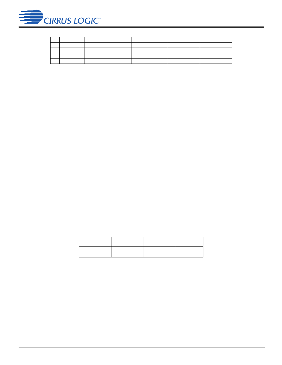
Table 4-6. ADSP Operational Mode and Pin Configurations
M/S SDOUT_3ST ADSP Operational Mode SDOUT Pin Driver LRCK Pin Driver SCLK Pin Driver
0
0
I
2
S Slave Mode
Output
Input
Input
0
1
I
2
S Slave Mode
Hi-Z
Input
Input
1
0
I
2
S Master Mode
Output
Output
Output
1
1
I
2
S Master Mode
Hi-Z
Output
Output
Table 4-7. ADSP Rates
MCLK
INT
Rate
(MHz)
LRCK Rate
(kHz)
f
MCLK(INT)
/f
LRCK
(Rate Ratio)
RATIO
6.0000
48.000
125
1
6.1440
48.000
128
0