Rainbow Electronics DS2172 User Manual
Page 5
DS2172
031197 5/20
PIN
DESCRIPTION
TYPE
SYMBOL
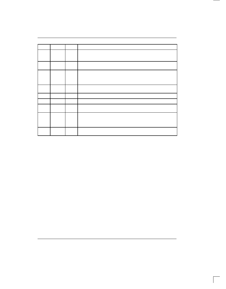
24
RL
I
Receive Load. A positive–going edge loads the previous 32 bits of data
received at RDATA into the Pattern Receive Registers. RL is logically OR’ed
with control bit PCR.3. Should be tied to V
SS
if not used.
25
RDATA
I
Receive Data. Received NRZ serial data, sampled on the rising edge of
RCLK.
26
RDIS
I
Receive Disable. Set high to prevent the data at RDATA from being
sampled. Set low to allow bits at RDATA to be sampled. Should be tied to V
SS
if not used. See Figure 6 for timing information. All receive side operations
are disabled when RDIS is high.
27
RCLK
I
Receive Clock. Input clock from transmission link. 0 to 52 MHz. Can be a
gapped clock. Fully independent from TCLK.
28
V
DD
–
Positive Supply. 5.0 volts.
29
V
SS
–
Signal Ground. 0.0 volts. Should be tied to local ground plane.
30
TCLK
I
Transmit Clock. Transmit demand clock. 0 to 52 MHz. Can be a gapped
clock. Fully independent of RCLK.
31
TDIS
I
Transmit Disable. Set high to hold the current bit being transmitted at
TDATA. Set low to allow the next bit to appear at TDATA. Should be tied to
V
SS
if not used. See Figure 7 for timing information. All transmit side opera-
tions are disabled when TDIS is high.
32
TDATA
O
Transmit Data. Transmit NRZ serial data, updated on the rising edge of
TCLK.