Rainbow Electronics DS2130Q User Manual
Page 5

DS2130Q
041295 5/22
HARDWARE RESET
RST allows the host to reset the DSP algorithms and
the contents of the serial port control registers. This pin
must be held low for at least 1 ms on system power-up
after MCLK is stable to ensure that the device has initial-
ized properly. RST clears all bits of both control regis-
ters except the CPD1 and CPD2 bits, which are set to
one. However, these bits are ignored until they have
been reset by the host; that is, the DS2130 will not pow-
er up in the power-down mode. This permits the host to
communicate through the serial port at full speed after
power-up.
SERIAL PORT CONTROL
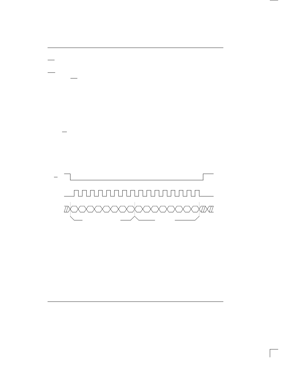
An external host controller writes configuration data to
the DS2130 via the serial port through inputs SCLK,
SDI, and CS as shown in Figure 2 (read operations are
not supported). Each write to the DS2130 is either a
2-byte write or a 4-byte write. A 2-byte write consists of
the Address/Command Byte (ACB) followed by a byte
to configure either the Voice Control Register (VCR) or
the Tone Control Register (TCR). The 4-byte write con-
sists of the ACB followed by a byte to configure the ap-
propriate control register and then two bytes for input
and output time slot mapping. When writing to the VCR,
the next two bytes program the input and output time
slots respectively for the compression/expansion (CPX)
side interface. When writing to the TCR , the next two
bytes program the input and output time slots respec-
tively for the PCM side interface.
ADDRESS/COMMAND BYTE
The address/command byte is the first byte written to
the serial port; it identifies which of the 64 possible
DS2130’s sharing the serial bus is to be accessed. Ad-
dress data must match that at inputs A0 to A5. If no
match occurs, the DS2130 ignores the following data at
SDI. If an address match occurs, the next three bytes
written are accepted as control, input and output time
slot data. Bit ACB.6 determines whether the Voice or
Tone Control register is to be updated.
SERIAL PORT WRITE Figure 2
SCLK
SDI
A0
A1
A2
A3
A4
A5
0
ADDRESS/COMMAND
CONTROL
CR7
CR0
V/T
CS
NOTE:
A 2-byte write is shown.
