Rainbow Electronics DS2130Q User Manual
Page 13

DS2130Q
041295 13/22
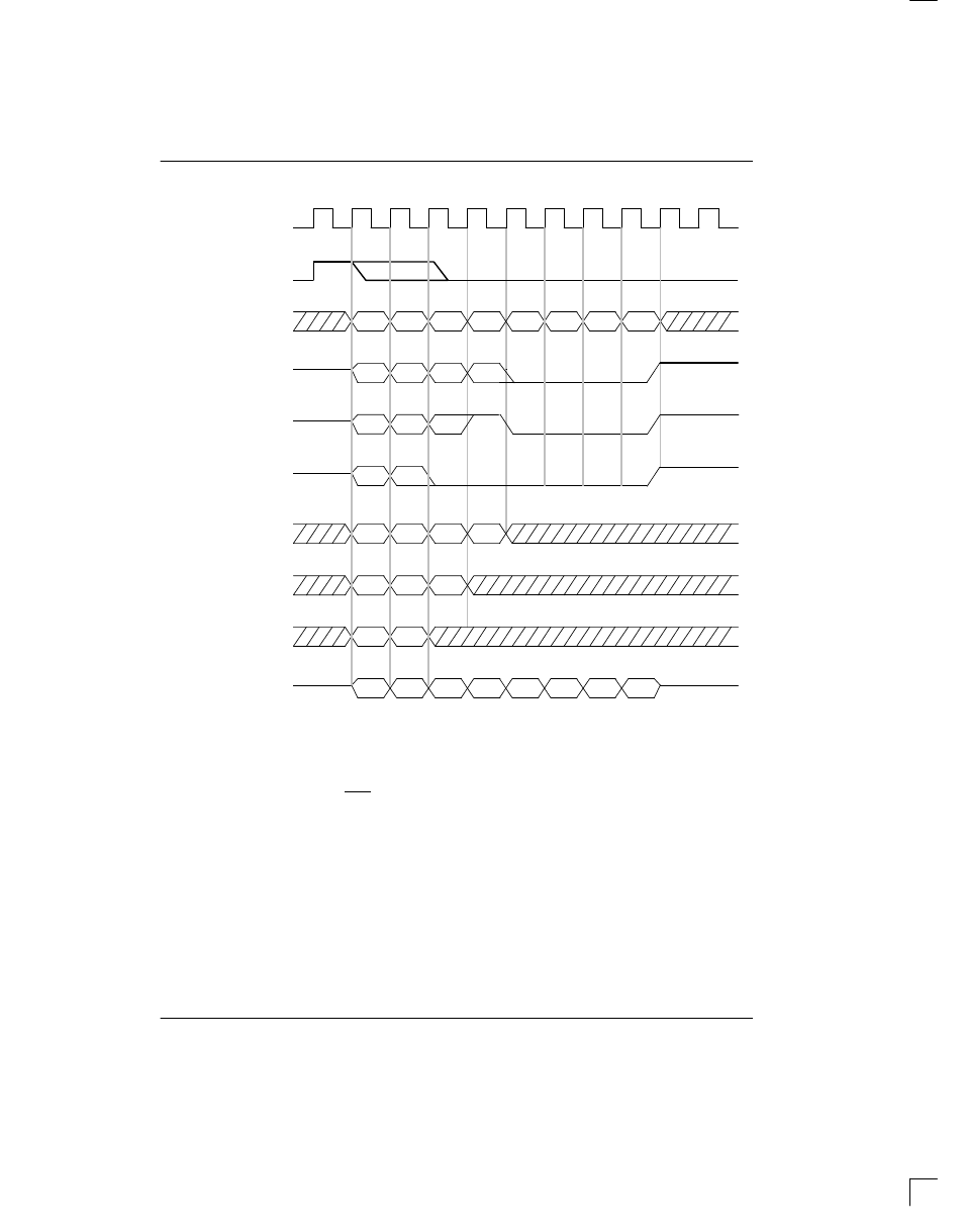
PCM/CPX I/O (CXS3=1) Figure 11
MSB
LSB
0
0
MSB
LSB
LSB
LSB
MSB
MSB
3–STATE
3–STATE
3–STATE
MSB
LSB
MSB
MSB
LSB
LSB
MSB
LSB
3–STATE
CPXOUT
CPXOUT
CPXOUT
PCMIN
CPXFS, PCMFS
PCMCLK,CPXCLK
CPXIN
CPXIN
CPXIN
PCMOUT
ЗЗЗЗЗ
ЗЗЗЗЗ
(CXS1=1,CSX2=1)
(CXS1=1,CSX2=1)
(CXS1=0,CSX2=0)
(CXS1=0,CSX2=1)
(CXS1=1,CSX2=1)
(CXS1=0,CSX2=1)
1
2
0
0
0
0
0
0
0
0
1
0
0
0
0
NOTES:
1. When CXS3=1, all CPX-side time slots are eight bits wide and CPXOUT data samples are repeated in the
next CPXFS frame sync during the same time slot. Therefore, only alternate data samples need to actually
be used for host processing.
2. When CXS3=1, all CPXIN data must be repeated in next frame sync (CPXFS).
INPUT TO OUTPUT DELAY
With all compression algorithms, the total delay from the
time the PCM data sample is captured by the DS2130 to
the time it is output is always less than 375
µ
s. The ex-
act delay is determined by the input and output time
slots selected for each channel.
ON-THE-FLY ALGORITHM SELECTION
The user can switch between the three available algo-
rithms on-the-fly. That is, the DS2130 does not need to
be reset or stopped to make the change from one algo-
rithm to another. However, the CXRST bit in the Voice
Control register must be set to a one when making the
algorithm change. The DS2130 reads the Control regis-
ter before it starts to process each PCM or CPX sample.
If the user wishes to switch algorithms, then the Voice
Control register must be updated via the serial port be-
fore the first input sample to be processed with the new
algorithm arrives at either PCMIN or CPXIN. PCM and
ADPCM outputs will tristate during register updates.
