Rainbow Electronics DS2130Q User Manual
Page 12

DS2130Q
041295 12/22
PCM AND CPX INPUT/OUTPUT
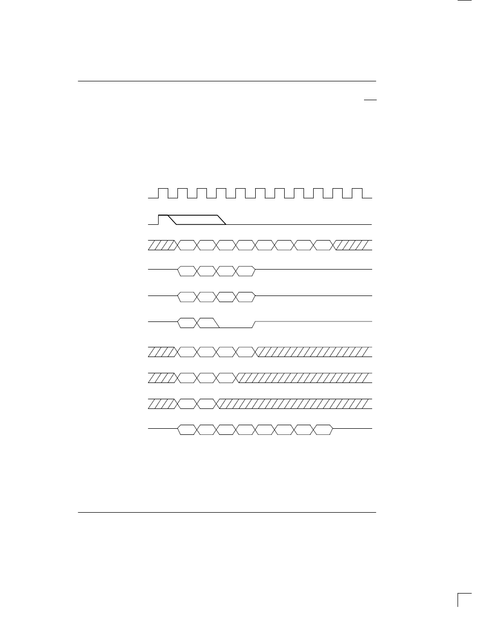
The organization of the CPX-side input and output time
slots on the DS2130 depends upon the state of bit CXS3
in the VCR. When CXS3=0, all time slots for CPXOUT
and CPXIN are four bits wide; when CXS=1,all time
slots are eight bits wide. Also, when CXS3=1, all
CPXOUT data is repeated in the next CPXFS sample;
therefore, only one out of every two CPXOUT samples
needs to be actually used. However, CPXIN data must
be repeated twice when CXS3=1.
PCM-side time slots are always eight bits wide, regard-
less of CXS3. Figure 10 demonstrates how the DS2130
handles the I/O when CXS3=0; Figure 11 likewise
shows the I/O when CXS3=1. It is assumed in both fig-
ures that the input and output time slots for both chan-
nels are set to zero.
PCM/CPX I/O (CXS3=0) Figure 10
MSB
LSB
0
0
MSB
LSB
LSB
LSB
MSB
MSB
3–STATE
3–STATE
3–STATE
MSB
LSB
MSB
MSB
LSB
LSB
MSB
LSB
3–STATE
CPXOUT
CPXOUT
CPXOUT
PCMIN
CPXFS, PCMFS
PCMCLK,CPXCLK
CPXIN
CPXIN
CPXIN
PCMOUT
(CXS1=0,CSX2=1)
(CXS1=1,CSX2=1)
(CXS1=0,CSX2=0)
(CXS1=0,CSX2=1)
(CXS1=1,CSX2=0)
(CXS1=0,CSX2=0)
1
ЗЗЗЗЗЗ
ЗЗЗЗЗЗ
NOTE:
1. The CPXFS and PCMFS frame sync pulses must be at least 1 CPXCLK or PCMCLK high.
