Max9489 multiple-output network clock generator, Chip information, Setting the clock frequencies – Rainbow Electronics MAX9489 User Manual
Page 9: Frequency margin control, Power supply, Board layout considerations
MAX9489
Multiple-Output Network Clock Generator
_______________________________________________________________________________________
9
Setting the Clock Frequencies
Each CLK_ output has an associated control register.
The contents of the registers determine the frequency
of their associated outputs. Table 3 provides the fre-
quency mapping for the registers.
Example: To program CLK3 to 80MHz, first address the
device with R/W low, then send register address byte
0x03 followed by data byte 0x05 (Figure 5).
Frequency Margin Control
Frequency margin is controlled through control register
0x10. Table 4 provides the mapping for the available
margins. A selected margin applies to all outputs.
Example: To increase all clock outputs by 5%, address
the device, then send register address byte 0x10 fol-
lowed by data byte 0x01.
Power Supply
The MAX9489 uses a 3.0V to 3.6V power supply con-
nected to V
DD
, and 3.0V to 3.6V connected to AV
DD
.
Bypass each V
DD
at the device with a 0.1µF capacitor.
Also bypass AV
DD
at the device with a 0.1µF capacitor.
Additionally, use a bulk bypass capacitor of 10µF
where power enters the circuit board.
Board Layout Considerations
As with all high-frequency devices, board layout is
critical to proper operation. Place the crystal as close
as possible to X1 and X2, and minimize parasitic
capacitance around the crystal leads. Ensure that the
exposed pad makes good contact with GND.
Chip Information
TRANSISTOR COUNT: 15,219
PROCESS: CMOS
SCL
MSB
1
SDA
1
A4
A3
A2
A1
A0
ACK
LSB
START
ACKNOWLEDGE
NOT ACKNOWLEDGE
R/W
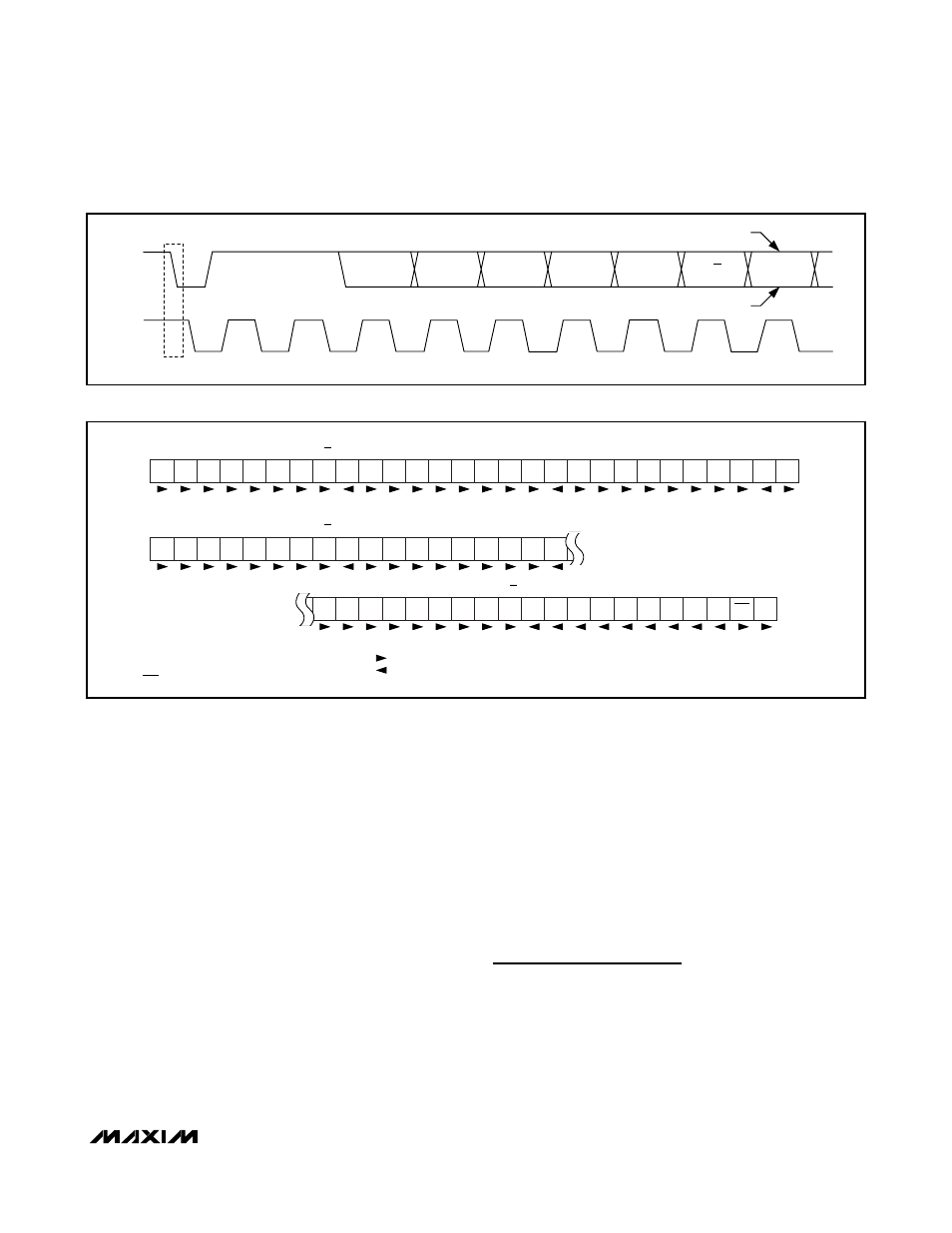
Figure 3. I
2
C Address and Acknowledge
S
1
1
A4
A3
A2
A1
0
ACK RA7 RA6 RA5 RA4 RA3 RA2 RA1 RA0 ACK
D7
D6
D5
D4
D3
D2
D1
D0
ACK
P
MASTER-WRITE DATA STRUCTURE
START
DEVICE ADDRESS
REGISTER ADDRESS
DATA IN
STOP
R/W
RS
1
1
A4
A3
A2
A1
A0
1
ACK
D7
D6
D5
D4
D3
D2
D1
D0
P
DEVICE ADDRESS
DATA OUT
STOP
R/W
S
1
1
A4
A3
A2
A1
0
ACK RA7 RA6 RA5 RA4 RA3 RA2 RA1 RA0 ACK
MASTER-READ DATA STRUCTURE
START
DEVICE ADDRESS
REGISTER ADDRESS
R/W
ACK
S = START CONDITION
A_ = DEVICE ADDRESS
ACK = ACKNOWLEDGE
ACK = NOT ACKNOWLEDGE
RA_ = REGISTER ADDRESS
D_ = DATA
P = STOP CONDITION
RS = REPEATED START
DATA DIRECTION
= MASTER TO SLAVE
= SLAVE TO MASTER
Figure 4. I
2
C Interface Data Structure